Register Transfer Level Hardware Description with Verilog:Sequential Circuits
Sequential Circuits
As with any digital circuit, a sequential circuit can be described in Verilog by the use of gates, Boolean expressions, or behavioral constructs (e.g., the always statement). While gate-level descriptions enable a more detailed description of timing and delays, because of complexity of clocking and register and flip-flop controls, these circuits are usually described by the use of procedural always blocks. This section shows the various ways sequential circuits are described in Verilog. The following discusses primitive structures like latch and flip-flops, and then generalizes coding styles used for representing these structures to more complex sequential circuits including counters and state machines.
Basic Memory Elements at the Gate Level
A clocked D-latch latches its input data during an active clock cycle. The latch structure retains the latched value until the next active clock cycle. This element is the basis of all static memory elements.
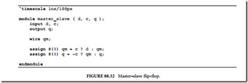
A simple description for a D-latch uses two cross-coupled NOR gate instantiations. Such a description is at the gate level and not very efficient in simulation. Alternatively, the same latch can be described with an assign statement as shown below.
This statement simply describes what happens in a latch. The statement says that when c is 1, the q output receives d, and when c is 0 it retains its old value. Using two such statements with complementary clock values a master–slave flip-flop is described. As shown in Figure 88.32, the qm net is the master output and q the flip-flop output.
This code uses two concurrent assign statements. As discussed before, these statements model logic structures with net-driven outputs (qm and q). The order in which the statements appear in the body of the master_slave module is not important.
Memory Elements Using Procedural Statements
Although latches and flip-flops can be described by primitive gates and assign statements, such descrip- tions are hard to generalize, and describing more complex register structures cannot be done this way. This section uses always statements to describe latches and flip-flops. We will show that the same coding styles used for these simple memory elements can be generalized to describe memories with complex control as well as functional register structures like counters and shift registers.
Latches
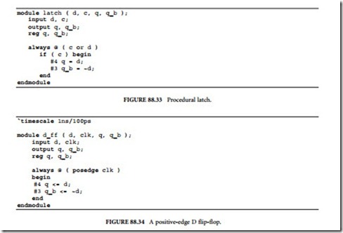
Figure 88.33 shows a D-latch described by an always statement. The outputs of the latch are declared as reg because they are being driven inside the always procedural block. Latch clock and data inputs (c and d) appear in the sensitivity list of the always block, making this procedural statement sensitive to
c and d. This means that when an event occurs on c or d, the always block wakes up and it executes all its statements in the sequential order from beginning to end.
The if-statement enclosed in the always block puts d into q when c is active. This means that if c is 1 and d changes, the change on d propagates to the q output. This behavior is referred to as transparency, which is how latches work. While clock is active, a latch structure is transparent, and input changes affect its output.
Any time the always statement wakes up, if c is 1, it waits 4 ns and then puts d into q. It then waits another 3 ns and then puts the complement of d into q_b. This makes the delay of the q_b output 7 ns.
D Flip-Flop
While a latch is transparent, a change on the D-input of a D flip-flops does not directly pass on to its output. The Verilog code of Figure 88.34 describes a positive-edge trigger D-type flip-flop.
The sensitivity list of the procedural statement shown includes posedge of clk. This always statement only wakes up when clk makes a 0 to 1 transition. When this statement does wake up, the value of d is put into q. Obviously, this behavior implements a rising-edge D flip-flop.
Instead of posedge, use of negedge would implement a falling-edge D flip-flop. After the specified edge, the flow into the always block begins. In our description, this flow is halted by 4 ns by the #4 delay-control statement. After this delay, the value of d is read and put into q. Following this transaction, the flow into the always block is again halted by 3 ns, after which ~d is put into qb. This makes the delay of q after the edge of the clock equal to 4 ns. The delay for q_b becomes the accumulation of the delay values shown, and it is 7 ns. Using nonblocking assignments (arrows in Figure 88.34) is recommended in clocked always statements.
Synchronous Control
The coding style presented for the above simple D flip-flop is a general one and can be expanded to cover many features found in flip-flops and even memory structures. The description shown in Figure 88.35 is a D-type flip-flop with synchronous set and reset (s and r) inputs.
The description uses an always block that is sensitive to the positive-edge of clk. When clk makes a 0 to 1 transition, the flow into the always block begins. Immediately after the positive-edge, s is inspected and if it is active (1), after 4 ns q is set to 1 and 3 ns after that q_b is set to 0. Following the positive-edge of clk, if s is not 1, r is inspected and if it is active, q is set to 0. If neither s nor r are 1, the flow of the program reaches the last else part of the if-statement and assigns d to q.
The behavior discussed here only looks at s and r on the positive-edge of clk, which corresponds to a rising- edge trigger D-type flip-flop with synchronous active high set and reset inputs. Furthermore, the set input is given a higher priority over the reset input. The flip-flop structure that corresponds to this description is shown in Figure 88.36.
Other synchronous control inputs can be added to this flip-flop in a similar fashion. A clock enable (en) input would only require inclusion of an if-statement in the last else part of the if-statement in the code of Figure 88.35. Note that delays such as those of this flip-flop are ignored in synthesis.
Asynchronous Control
The control inputs of the flip-flop of Figure 88.35 are synchronous because the flow into the always statement is only allowed to start when the posedge of clk is observed. To change this to a flip-flop with asynchronous control, it is only required to include asynchronous control inputs in the sensitivity list of its procedural statement.
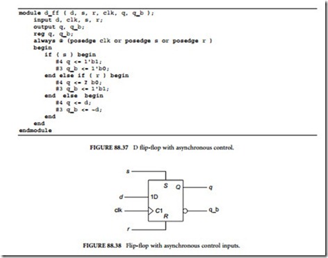
Figure 88.37 shows a D flip-flop with active high asynchronous set and reset control inputs. Note that the only difference between this description and the code of Figure 88.35 (synchronous control) is the inclusion of posedge s and posedge r in the sensitivity list of the always block. This inclusion allows the flow into the procedural block to begin when clk becomes 1 or s becomes 1 or r becomes 1. The if-statement in this block checks for s and r being 1, and if none are active (activity levels are high) then clocking d into q occurs.
An active high (low) asynchronous input requires inclusion of posedge (negedge) of the input in the sensitivity list, and checking its 1 (0) value in the if-statement in the always statement. Furthermore, clocking activity in the flip-flop (assignment of d into q) must always be the last choice in the if-statement of the procedural block.
The graphic symbol corresponding to the flip-flop of Figure 88.37 is shown in Figure 88.38.
Registers, Shifters, and Counters
Registers, shifter-registers, counters and even sequential circuits with more complex functionalities can be described by simple extensions of the coding styles presented for the flip-flops. In most cases, the functionality of the circuit only affects the last else of the if-statement in the procedural statement of codes shown for the flip-flops.
Registers
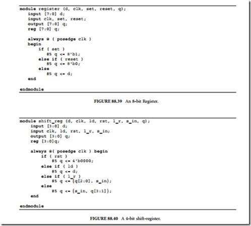
Figure 88.39 shows an 8-bit register with synchronous set and reset inputs. The set input puts all 1s in the register and the reset input resets it to all 0s. The main difference between this and the flip-flop with synchronous control is the vector declaration of inputs and outputs.
Shift-Registers
A 4-bit shift-register with right- and left-shift capabilities, a serial-input, synchronous reset input, and parallel loading capability is shown in Figure 88.40. As shown, only the positive-edge of clk is included in the sensitivity list of the always block of this code, which makes all activities of the shift-register synchronous with the clock input. If rst is 1, the register is reset, if ld is 1 parallel d inputs are loaded
into the register, and if none are 1 shifting left or right takes place depending on the value of the l_r input (1 for left, 0 for right). Shifting in this code is done by use of the concatenation operator { }. For left-shift, s_in is concatenated to the right of q[2:0] to form a 4-bit vector that is put into q. For right-shift, s_in is concatenated to the left of q[3:1] to form a 4-bit vector that is clocked into q[3:0]. As before, delay values are only used for simulation and do not synthesize.
The style used for coding this register is the same as that used for flip-flops and registers presented earlier. In all these examples, a single procedural block handles function selection (e.g., zeroing, shifting, or parallel loading) as well as clocking data into the register output.
Another style of coding registers, shift-registers and counters is to use a combinational procedural block for function selection and another for clocking.
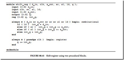
As an example, consider a shift-register that shifts s_cnt number of places to the right or left depending on its sr or sl control inputs (Figure 88.41). The shift-register also has an ld input that enables its clocked parallel loading. If no shifting is specified, i.e., sr and sl are both zero, then the shift register retains its old value. The Verilog code of Figure 88.41 shows two procedural blocks that are identified by combinational and register. A block name appears after the begin keyword that begins a block and is separated from this keyword by use of a colon.
The combinational block is sensitive to all inputs that can affect the shift-register output. These include the parallel d_in, the s_cnt shift-count, sr and sl shift-control inputs, and the ld load-control input. In the body of this block an if-else statement decides on the value placed on the int_q internal variable. The value selection is based on values of ld, sr, and sl. If ld is 1, int_q becomes d_in that is the parallel input of the shift register. If sr or sl is active, int_q receives the previous value of int_q shifted to right or left as many as s_cnt
places. In this example, shifting is done by the use of >> and << operators. On the left, these operators take the vector to be shifted, and on the right they take the number of places to shift.
The int_q variable that is being assigned values in the combinational block is a 4-bit reg that connects the output of this block to the input of the register block.
The register block is a sequential block that handles clocking int_q into the shift-register output. This block (as shown in Figure 88.41) is sensitive to the positive edge of clk and its body consists of a single reg assignment. As before, we use nonblocking assignments for variables that represent registers.
Note in this code that both q and int_q are declared as reg because they are both receiving values in procedural blocks.
Counters
Any of the styles described for the shift-registers in the previous discussion can be used for describing counters. A counter counts up or down, while a shift-register shifts right or left. We use arithmetic operations in counting as opposed to shift or concatenation operators in shift-registers.
Figure 88.42 shows a 4-bit up-down counter with a synchronous rst reset input. The counter has an ld input for doing the parallel loading of d_in into the counter. The counter output is q and it is declared as reg since it is receiving values within a procedural statement.
Discussion about synchronous and asynchronous control of flip-flops and registers also apply to the counter circuits. For example, inclusion of posedge rst in the sensitivity list of the counter of Figure 88.42 would make its resetting asynchronous.
State Machine Coding
Coding styles presented so far can be further generalized to cover finite state machines of any type. This section shows coding for Moore and Mealy state machines. The examples we will use are simple sequence detectors. These circuits represent the controller part of a digital system that has been partitioned into a data path and a controller.
Moore Detector
State diagram for a Moore sequence detector detecting 101 on its x input is shown in Figure 88.43. The machine has four states that are labeled: reset, got1, got10, and got101. Starting in reset, if the 101 sequence is detected, the machine goes into the got101 state in which the output becomes 1. In addition to the x input, the machine has a rst input that forces the machine into its reset state. The resetting of the machine is synchronized with the clock.
The Verilog code of the Moore machine of Figure 88.43 is shown in Figure 88.44. After the declaration of inputs and outputs of this module, parameter declaration declares four states of the machine as 2-bit parameters. The square-brackets following the parameter keyword specify the size of parameters being declared. Following parameter declarations in the code of Figure 88.44, the two-bit current reg type variable is declared. This variable holds the current state of the state machine.
The always block used in the module of Figure 88.44 describes state transitions of the state diagram of Figure 88.43. The main task of this procedural block is to inspect input conditions (values on rst and x) during the present state of the machine defined by current and set values into current for the next state of the machine. The flow into the always block begins with the positive edge of clk. Since all activities in this machine are synchronized with the clock, only clk appears on the sensitivity list of the always block. Upon entry into this block, the rst input is checked and if it is active, current is set to reset (reset is a declared parameter and its
value is 0). The value put into current in this pass through the always block gets checked in the next pass with the next edge of the clock. Therefore this assignment is regarded as the next-state assignment. When this assignment is made, the if-else statements skip the rest of the code of the always block, and this always block will next be entered with the next positive edge of clk. An assignment statement outside of the always block is used for assigning values to the z output of the circuit. As shown here and as shown in the state diagram of this machine, the output becomes 1 when the current variable is got101.
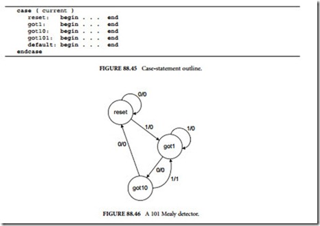
Upon entry into the always block, if rst is not 1, program flow reaches the case statement that checks the value of current against the four states of the machine. Figure 88.45 shows an outline of this case-statement. This statement has five case-alternatives. A case-alternative is followed by a block of statements bracketed by the begin and end keywords. In each such block, actions corresponding to the active state of the machine are taken. The default case alternative is taken when none of the other alternatives are true. This part is useful for avoiding unwanted latches in synthesis.
In this coding style, for every state of the machine there is a case-alternative that specifies the next state values. For larger machines, there will be more case-alternatives, and more conditions within an alternative. Otherwise, this style can be applied to state machines of any size and complexity.
This same machine can be described in Verilog in many other ways. We will show alternative styles of coding state machines by use of examples that follow.
A Mealy Machine Example
Unlike Moore machines the outputs of which are only determined by the current state of the machine, a Mealy machine, the outputs are determined by the state the machine is in as well as the inputs of the
circuit. This makes Mealy outputs not fully synchronized with the circuit clock. In the state diagram of a Mealy machine the outputs are specified along the edges that branch out of the states of the machine. Figure 88.46 shows a 101 Mealy detector. The machine has three states, reset, got1, and got10. While in got10, if the x input becomes 1 the machine prepares to go to its next state with the next clock. While waiting for the clock, its output becomes 1. While on the edge that takes the machine out of got10, if the clock arrives the machine goes into the got1 state. This machine allows overlapping sequences. The machine has no external resetting mechanism. A sequence of two zeros on input x puts the machine into the reset state in a maximum of two clocks.The Verilog code of the 101 Mealy detector is shown in Figure 88.47. After input and output declarations, a parameter declaration defines bit patterns (state assignments) for the states of the machine. Note here that state value 3 or binary 11 is unused. As in the previous example, we use the current two-bit reg to hold the current state of the machine.
After the declarations, an initial block sets the initial state of the machine to reset. This procedure for initializing the machine is only good for simulation and is not synthesizable.
This example uses an always block for specifying state transitions and a separate statement for setting values to the z output. The always statement responsible for state transitions is sensitive to the circuit clock and has a case statement that has case alternatives for every state of the machine. Consider, for example, the got10 state and its corresponding Verilog code segment, as shown in Figure 88.48.
The always statement used here specifies the next states of the machine based on conditions of the input and present state. Notice in this code segment that the case alternative shown does not have begin and end bracketing. Actually, begin and end keywords do not appear in blocks following if and else keywords either. Verilog only requires begin and end bracketing if there is more than one statement in a block. The use of this bracketing around one statement is optional. Since the if part and the else part each only contain one statement, begin and end keywords are not used. Furthermore, since the entire if-else statement reduces to only one statement, the begin and end keywords for the case-alternative are also eliminated.
The last case-alternative shown in Figure 88.47 is the default alternative. When checking current against all alternatives that appear before the default statement fail, this alternative is taken. There are several reasons that we use this default alternative. One is that, our machine only uses three of the possible four 2-bit assignments and 11 is unused. If the machine ever begins in this state, the default case makes reset the next state of the machine. The second reason why we use default is that Verilog assumes a four-value logic system that includes Z and X. If current ever contains a Z or X, it does not match any of the defined case alternatives, and the default case is taken. Another reason for use of default is that our machine does not have a hard reset and we are making provisions for it to go to the reset state. The last reason for default is that it is just a good idea to have it.
The last statement in the code fragment of Figure 88.55 is an assign statement that sets the z output of the circuit. This statement is a concurrent statement and is independent of the always statement above it. When current or x changes, the right-hand side of this assignment is evaluated and a value of 0 or 1 is assigned to z. Conditions on the right-hand side of this assignment are according to values put in z in the state diagram of Figure 88.47. Specifically, the output is 1 when current is got10 and x is 1, otherwise it is 0. This statement implements a combinational logic structure with current and x inputs and z output.
Huffman Coding Style
The Huffman model for a digital system characterizes it as a combinational block with feedbacks through an array of registers. Verilog coding of digital systems according to the Huffman model uses an always statement for describing the register part and another concurrent statement for describing the combinational part.
We will describe the state machine of Figure 88.43 to illustrate this style of coding. Figure 88.49 shows the combinational and register part partitioning that we will use for describing this machine. The combinational block uses x and p_state as input and generates z and n_state. The register block clocks n_state into p_state, and reset p_state when rst is active.
Figure 88.50 shows the Verilog code of Figure 88.43 according to the partitioning of Figure 88.49. As shown, parameter declaration declares the states of the machine. Following this declaration, n_state and p_state variables are declared as two-bit regs that hold values corresponding to the states of the 101 Moore detector. The combinational always block follows this reg declaration. Since this is a purely combinational block, it is sensitive to all its inputs, namely x and p_state. Immediately following the block heading, n_state is set to its inactive or reset value. This is done so that this variable is always reset with the clock to make sure it does retain its old value. As discussed before, retaining old values implies latches, which is not what we want in our combinational block.
The body of the combinational always block of Figure 88.50 contains a case-statement that uses the p_state input of the always block for its case-expression. This expression is checked against the states of the Moore machine. As in the other styles discussed before, this case-statement has case-alternatives for reset, got1, got10, and got101 states.
In a block corresponding to a case-alternative, based on input values, n_state and z output are assigned values. Unlike the other styles where current is used both for the present and next states, here we use two different variables, p_state and n_state.
The next procedural block shown in Figure 88.50 handles the register part of the Huffman model of Figure 88.49. In this part, n_state is treated as the register input and p_state as its output. On the positive edge of the clock, p_state is either set to the reset state (00) or is loaded with contents of n_state. Together,
combinational and register blocks describe our state machine in a very modular fashion. As in the other coding style done for this machine, an assign statement handles the assignment of values to the circuit output.
The advantage of this style of coding is in its modularity and defined tasks of each block. State transitions are handled by the combinational block and clocking is done by the register block. Changes in clocking, resetting, enabling, or presetting the machine only affect the coding of the register block. If we were to change the synchronous resetting to asynchronous, the only change we had to make was adding posedge rst to the sensitivity list of the register block.
The examples discussed above, in particular, the last style, show how combinational and sequential coding styles can be combined to describe very complex digital systems.
Memories
Verilog allows description and use of memories. Memories are described as arrays of vectors of variables and are declared as reg. Verilog allows reg data types for memories. Figure 88.51 shows a reg declaration declaring mem and its corresponding block diagram. This figure also shows several valid memory operations.
Operations shown here comply with Verilog 1999 and not Verilog 2001. More advanced features of Verilog 2001 are described in Chapter 90.
Square brackets that follow the reg keyword specify the word-length of the memory. The square brackets that follow the name of the memory (mem), specify its address space. A memory can be read by addressing it within its address range, e.g., mem[956]. Part of a word in a memory cannot be read directly, i.e., slicing a memory word is not possible. To read part of a word, the whole word must first be read in a variable and then slicing done on this variable. For example, data[7:4] can be used after a memory word has been placed into data.
With proper indexing, a memory word can be written into by placing the memory name and its index on the left-hand side of an assignment, e.g., mem[932] = data;, memories can also be indexed by reg or net type variables, e.g., mem[addr], when addr is a 10-bit address bus. Writing into a part of the memory is not possible. In all cases data directly written into a memory word affects all bits of the word being written into. For example to write the four-bit short_data into a location of mem, we have to decide what goes into the other four bits of the memory word.
Figure 88.52 shows a memory block with separate input and output buses. Writing into the memory is clocked, while reading from it only requires rw to be 1. An assign statement handles reading and an always block performs writing into this memory.





Comments
Post a Comment