COMPUTER-AIDED DESIGN (CAD) TOOLS FOR LAYOUT:PLANNING TOOLS
PLANNING TOOLS
There needs to be a planning phase for all layout design tasks, but in general a floorplan starts from the chip level down to the block level. The idea behind this methodology is to build everything bottom-up while using the top-level floorplan to define the block interfaces and to coordinate updates to these interfaces as portions of the design are completed or verified.
Chip Floorplanning Tools
Floorplanning is the process of identifying structures that should be placed together and allocating space for them so as to meet the conflicting goals of avail- able space (cost of the chip), required performance, and the desire to have every block connect seamlessly to everything else.
In most chips, the smallest design is also the highest performance design. Therefore, area and speed are characteristics that go hand-in-hand. A block or chip that is small in area has shorter interconnect lines, less routing, faster end-to-end signal paths, and even faster and more consistent place-and-route times.
Floorplanning is methodology that should result in a smaller design because the design is planned efficiently by combining the expertise of the layout designer in partitioning the circuitry and the optimization algorithms in the floorplanning tool.
Figure 10.2 shows the different components of a floorplan at the start of the design process.
To understand the role of a floorplan and how a tool can help the designer to obtain fast and correct results, it is important to understand the concepts and issues that a floorplanning tool is trying to address. A floorplanning tool does the following:
• Understands the different partitions or blocks of a design
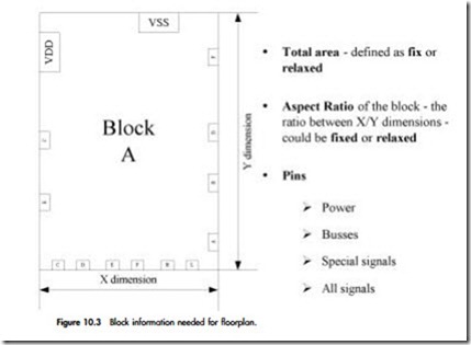
• Understands the critical characteristics of each of the blocks: size, aspect ratio, and pins
• Dynamically displays the connectivity between blocks and connections to the pads
• Allocates space for routing based on number of routing layers
• Places top-level ports based on constraints
• Places each block and optimizes the pin locations for each block based on the overall connectivity requirements and the feasibility of routing the signals between blocks
• Allows the user to make incremental modifications to the plan or to replan altogether Figure 10.3 highlights the important information on a block that is required before it can be instantiated in the chip-level floorplan.
Figure 10.4 outlines a procedure for using a floorplanner effectively. Here are some important hints to remember when using a floorplanning tool:
• Initially, all pads at the top level are assigned to be connected to a single layer. This constraint affects the router in its ability to optimize the connections to the pads. In some cases the pads can be assigned to two layers, which gives the router more freedom. In the case of many available layers (up to 10!), the assignment of pads to routing layers is best left to the layout designer and assigned manually. There may be dedicated layers for some ports that need to be assigned, such as power supplies and clocks.
• Block pins may have to be manually assigned to the correct layer as in the previous case.
• Inserting spare logic and signals is tricky. Typically, the netlist of a design does not contain spare elements, so these elements need to be inserted manually as well. The person using the tool should learn how to “massage” the netlist by introducing “fictional” lines and pins, enlarging blocks for spare logic, and adding dummy blocks that will be used for spare logic. Proper placement of the spare elements is also necessary to ensure that the spare lines are close to the spare logic so they can be used easily.
• Blocks that are subject to change should be placed strategically where there might be extra space for the block to grow in size.
Block Floorplanning Tools
At the block level, the procedure for floorplanning is fundamentally the same as the chip floorplanning procedure, with minor exceptions. Instead of working with blocks, the floorplanner works with groups of cells that are defined based on the functionality and connectivity of the design. In this case the design is more mature, in that the design is better defined with cells and connections and there are fewer empty blocks with unknown contents.
In comparison to chip floorplanning, block-level floorplanning has the fol- lowing similarities and differences:
• At the block level there may be thousands of cells; at the chip level the number is usually less than 20
• Port handling is similar, although there may be many more ports
• The pins in a block can number in the hundreds of thousands, and the connectivity is much more complex than at the chip level
• If the process has more than three layers of metal, the floorplan may not have channels at all—the plan will look like a sea of cells
• In the case where there are imported or hard cores, the floorplanner will optimize their placement among the rest of the logic.
Floorplanners need to export information based on the design needs or the overall design flow being used for the design. Figure 10.5 illustrates the data formats that a floorplanner provides. The different formats depend on the target application.


Comments
Post a Comment