SRAM:Decoder and Word-Line Decoding Circuit [10–13].
Decoder and Word-Line Decoding Circuit [10–13]
Two kinds of decoders are used in SRAM: the row decoder and the column decoder. Row decoders are needed to select one row of word-lines out of a set of rows in the array. A fast decoder can be implemented by using AND/NAND and OR/NOR gates. Figure 52.7 shows the schematic diagrams of static and dynamic AND gate decoders. The static NAND-type structure is chosen due to its low power consumption, that is, only the decoded row transitions. The dynamic structure is chosen due to its speed and power improvement over conventional static NAND gates.
From a low-voltage operation standpoint, a dynamic NOR-base decoding would provide lower delay times through the decoder due to the limited amount of stacking of devices. Figure 52.8 shows circuit diagrams of dynamic NOR gates. The dynamic CMOS gate as shown in Figure 52.8(a) consists of input- NMOSs whose drain nodes are precharged to a high level by a PMOS when a clock signal Φ is at a low level, and conditionally discharged by the input-NMOSs when a clock signal Φ is at a high level. The delay time of the dynamic NOR/OR gate does not increase when the number of input signals increases. This is because only one PMOS and two NMOSs are connected in series, even if the number of input signals is large. However, the output of the OR signal is slower than that of the NOR signal because the OR signal is generated from the inverter driven by the NOR signal.
Figure 52.8(b) shows the source-coupled-logic (SCL) [11] NOR/OR circuit. When a clock signal Φ is at a low level, the drain nodes of the NMOS (N1, N2) are precharged to a high level in the circuit. If at least one of input signals of the circuit is at a high level and the clock Φ then turns to a high level, node N1 is discharged to a low level and node N2 remains at a high level. On the other hand, if all the input signals are at a low level and Φ then turns to a high level, node N2 is discharged and node N1 remains at a high level. The SCL circuit can produce an OR signal and a NOR signal simultaneously. Thus, the SCL circuit is suitable for predecoders that have a large number of input signals and for address buffers that need to produce OR and NOR signals simultaneously.
Column decoders select the desired bit pairs out of the sets of bit pairs in the selected row. A typical dynamic AND gate decoder as shown in Figure 52.7(b) can be used for column decoding because the AND structure meets the delay requirements (column decode is not in the worst-case delay path) and does so at a much lower power consumption.
A highly integrated SRAM adopts a multi-divided memory cell array structure to achieve high-speed word decoding and reduce column power dissipation. For this purpose, many high-speed word-decoding circuit architectures have been proposed, such as divided word-line (DWL) [8] and hierarchical word decoding (HWD) [9] structures. The multi-stage decoder circuit technique is adopted in both word- decoding circuit structures to achieve high-speed and low-power operation. The multi-stage decoder circuit has advantages over the one-stage decoder in reducing the number of transistors and fanin. Also, it reduces the loading on the address input buffers. Figure 52.9 shows the decoder structure for a typical partitioned memory array with divided word-line (DWL). The cell array is divided into NB blocks. If the SRAM has NC columns, each block contains NC /NB columns. The divided word-line in each block is activated by the global word-line and the vertical block select line. Consequently, only the memory cells connected to one divided word-line within a selected block are accessed in a cycle. Hence, the column current is reduced because only the selected columns switch. Moreover, the word-line selection delay, which is the sum of the global word-line delay and the divided word-line delay, is reduced. This is because the total capacitance of the global word-line is smaller than that of a conventional word-line. The delay time of each divided word-line is small due to the short length. In the block decoder, an additional signal Φ, which is generated from an ATD pulse generator, can be adopted to enable the decoder and ensure the pulse activated word-line.
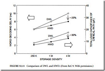
However, in high-density SRAM, with a capacity of more than 4 Mb, the number of blocks in the DWL structure will have to increase. Therefore, the capacitance of the global word-line will increase and that causes the delay and power to increase. To solve this problem, the hierarchical word decoding (HWD) [9] circuit structure, as shown in Figure 52.10, was proposed. The word-line is divided into multi-levels. The number of levels is determined by the total capacitance of the word select line to efficiently distribute it. Hence, the delay and power are reduced. Figure 52.11 shows the delay time and the total capacitance of the word decoding path comparison for the optimized DWL and HWD structures of 256-Kb, 1-Mb, and 4-Mb SRAMs.


Comments
Post a Comment