SRAM:Read/Write Operation
Read/Write Operation
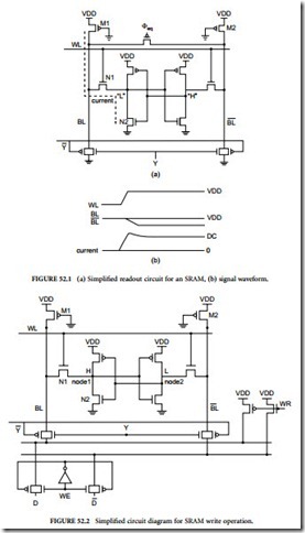
Figure 52.1 shows a simplified readout circuit for an SRAM. The circuit has static bit-line loads composed of pull-up PMOS devices M1 and M2. The bit-lines are pulled up to VDD by bit-line load transistors M1 and M2. During the read cycle, one word-line is selected. The bit line BL is discharged to a level determined by the bit-line load transistor M1, the accessed transistor N1, and the driver transistor N2 as shown in Figure 52.1(b). At this time, all selected memory cells consume a dc column current flowing through the bit-line load transistors, accessed transistors, and driver transistors. This current flow increases the operating power and decreases the access speed of the memory.
Figure 52.2 shows a simplified circuit diagram for SRAM write operation. During the write cycle, the input data and its complement are placed on the bit-lines. Then the word-line is activated. This will force the memory cell to flip into the state represented on the bit-lines, whereas the new data is stored in the memory cell. The write operation can be described as follows. Consider a high voltage level and a low voltage level are stored in both node 1 and node 2, respectively. If the data is to be written into the cell, then node 1 becomes low and node 2 becomes high. During this write cycle, a dc current will flow from VDD through bit-line load transistor M1 and write circuits to ground. This extra dc current flow in write cycle increases the power consumption and degrades the write speed performance. Moreover, in the tail portion of write cycle, if data 0 has been written into node 1 as shown in Figure 52.2, the turn-on word- line transistor N1 and driver transistor N2 form a discharge circuit path to discharge the bit-line voltage. Thus, the write recovery time is increased. In high-speed SRAM, write recovery time is an important component of the write cycle time. It is defined as the time necessary to recover from the write cycle to the read state after the WE signal is disabled [1]. During the write recovery period, the selected cell is in the quasi-read condition [2], which consumes dc current as in the case of read cycle.
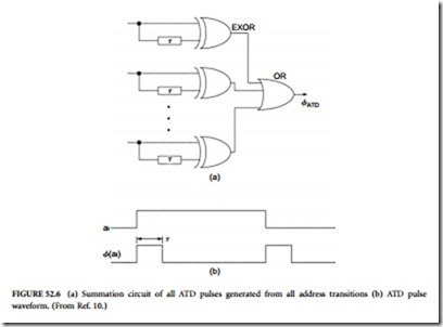
Based on the above discussion, the dc current problems that occur in the read and write cycles should be overcome to reduce power dissipation and improve speed performance. Some solutions for the dc current problems of conventional SRAM will be described. During the active mode (read cycle or write cycle), the word-line is activated, and all selected columns consume a dc current. Thus, the word-line activation duration should be shortened to reduce the power consumption and improve speed performance during the active mode. This is possible by using the Address Transition Detection (ATD) technique [3] to
generate the pulsed word-line signal with enough time to achieve the read and write operation, as shown in Figure 52.3.
However, the memory cells asserted by the pulsed word-line signal still consume dc current from VDD through bit-line load transistors, accessed transistors, and driver transistors or write circuits to the ground during the word-line activation period. A dynamic bit-line loads circuit technique [2,4–6] can be used to eliminate the dc power consumption during operation period.
Figure 52.4 shows a simplified circuit configuration and time diagram for read and write operation. In the read cycle, the bit-line load transistors are turned off because the ΦLD signal is in the high state. The bit-line load consists of only the stray capacitance. Therefore, the selected memory cell can rapidly drive the bit-line load, resulting in a fast access time. Moreover, the dc column current consumed by the other activated memory cells can be eliminated. Similarly, the dc current consumption in the write cycle can be eliminated.
A memory cell’s readout current Icell depends on the channel conductance of the transfer gates in a memory cell. As the supply voltage is scaled down, the speed performance of SRAM is decreased, significantly, due to small cell’s readout current. To increase the channel conductance, widening the channel width and/or boosting word-line voltage are used. For low-voltage operation, boosting the word- line voltage is effective in shortening the delay time, in contrast to widening the channel width. However,
this causes an increased power dissipation and a large transition time due to enhanced bit-line swing. To solve these problems, a step-down boosted-word-line scheme that shortens the readout time with little power dissipation penalty was reported by Morimura and Shibata in 1998 [7].
The concept of this scheme is shown in Figure 52.5(b), in contrast to the conventional full-boosted- word-line scheme in Figure 52.5(a). The step-down boosted-word-line scheme also boosts the selected word-line, but the boosted period is restricted only at the beginning of memory cell access. This enables the sensing operation to start early, by fast bit-line transition. During the sensing period of bit-line signals, the word-line potential is stepped down to the supply voltage to suppress the power dissipation; the reduced bit-line signals are sufficient to read out data by current sensing, and the reduced bit-line swing is effective in shortening the bit-line transition time in the next read cycle (Figure 52.5(c)). As a result, fast readout is accomplished with little dissipation penalty (Figure 52.5(d)).
The step-down boosted-word-line scheme is also used in data writing. In the writing cycle, the proposed scheme is just as effective in reducing the memory-cell current because the memory cells unselected by column-address signals consume the same power as in the read cycle. The boosted word-line voltage shortens the time for writing data because it increases the channel conductance of the access transistor in the selected memory cells. The writing recovery operation starts after the word-line voltage is stepped
down. Reducing the memory cell’s current accelerates the recovery operation of lower bit-lines. So, a shorter recovery time than that of the conventional full-boosted-word-line scheme is obtained.
Other circuit techniques for dc column current reduction, such as divided word-line (DWL) [8] and hierarchical word decoding (HWD) [9] structures will be described in the following sections.


Comments
Post a Comment