Emitter-Coupled Logic:Modification of Standard ECL Logic Gates with Wired Logic.
Modification of Standard ECL Logic Gates with Wired Logic
More complex logic functions than the output functions of the standard ECL logic gate shown in Figure 38.1 can be realized by changing the internal structures of the standard ECL logic gates. In other words, if we connect points inside one ECL gate to some points of another ECL gate, we can realize a complex logic function with a simpler electronic circuit configuration. In other words, we can realize logic functions by freely connecting transistors, resistors, and diodes, instead of regarding the fixed connection configuration of transistors, resistors, and diodes as logic gates whose structure cannot be changed. This approach could be called transistor-level logic design. Wired logic is a powerful means for this, and collector-dotting and emitter-dotting are the basic techniques of wired logic.
Collector-Dotting
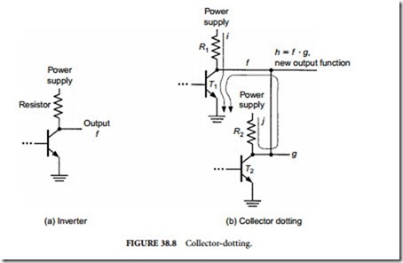
Collector-dotting is commonly used in bipolar transistor circuitry to realize the Wired-AND operation. Suppose we have the inverter circuit shown in Figure 38.8(a) as part of an ECL logic gate. Its output function, f, at the collector of the bipolar transistor is 1 when the voltage at the collector is high, and f is 0 when the voltage at the collector is low. Then, suppose there is another like circuit whose output function at the collector is g. If the collectors of these two circuits, instead of the emitters for emitter-dotting in Figure 38.4(b), are tied together as shown in Figure 38.8(b), the new output function at the tied
point is h = f ⋅ g, replacing the original functions, f and g. This connection is called collector-dotting, realizing Wired-AND. The tied point represents the new function f ⋅ g because if one of T1 and T2, or both is conductive in Figure 38.8(b), the voltage at the tied point is low; otherwise (i.e., only when both transistors, T1 and T2, are non-conductive), the voltage at the tied point can be high.
In Figure 38.9(a), Figure 38.2 is repeated as gate 1 and gate 2. Transistor Tx has input x at its base, and its collector represents function x if Ty does not exist because when its base has a low voltage (i.e., logic value 0), its collector has a high voltage (i.e., logic value 1) and vice versa. Similarly, the collector of transistor Ty represents y , if Tx does not exist. Then by tying together these collectors (i.e., collector- dotting), the tied point (i.e., point A) represents x ⋅ y = x ∨ z, as already explained with respect to Figure 38.2. Notice that the collector of Tx and the collector of Ty do not represent the original functions x and y respectively, after collector-dotting. Since the voltage level at B is always opposite to that at A, point B represents x ∨ y.
We can use collector-dotting more freely. Point A in gate 1 in Figure 38.9(a) can be connected to point A′ or B′ in gate 2. Point B can also be connected to point A′ or B′. Such connections realize Wired-AND or collector-dotting. By collector-dotting points B and B′ as shown in Figure 38.9(b), point B 7 (also B′) represents new function (x ∨ y) ⋅ (z ∨ w), which also appears at the emitter of transistor T. After this collector-dotting, points B and B′ do not represent the original functions x ∨ y and z ∨ w, respectively, anymore. Also, note that the function at any point that is not collector-dotted, such as A and A′, is unchanged by collector-dotting of B and B′. In Figure 38.9(b), two transistors, two diodes, and resistors (shown in the dotted line) are added for adjustment of voltage and current. But they have nothing to do with logic operations.
Another example is the parity function xy ∨ xy realized by connecting two ECL gates as shown in Figure 38.10. The parity function requires four ECL gates if designed with the standard ECL logic gates as shown in Figure 38.10(c), but can be realized by the much simpler electronic circuit of Figure 38.10(b). In other words, xy and xy are realized by Wired-AND, then these two products are Wired-ORed in order to realize xy ∨ xy. In Figure 38.10 as well as Figure 38.9, some resistors or transistors may be necessary for electronic performance improvement (since resistors R1 and R2 draw too much current in gate 1 in Figure 38.10(a), new resistors are added in Figure 38.10(b) in order to clamp the currents), and unnecessary resistors or transistors may be deleted, although such an addition or elimination of resistors or transistors has nothing to do with logic operations.


Comments
Post a Comment