ROM/PROM/EPROM:PROM
PROM
Since process technology has shifted to QLM or PLM to achieve better device performance, it is important to develop a ROM technology that offers short TAT, high density, high speed, and low power. There are many types of ROM each with merits and demerits [5]:
The diffusion programming ROM has excellent density but has a very long process cycle time. The conventional VIA-2 contact programming ROM has better cycle time, but it has poor density.
An architecture VIA-2 contact programming ROM for QLM and PLM processes has simple processing with high density which obtains excellent results targeting 2.5 V and 2.0 V supply voltage.
Read Only Memory Module Architecture
The details of the ROM module configuration are shown in Figure 51.4. This ROM has a single access mode (16-bit data read from half of ROM array) and a dual access mode (32-bit data read from both ROM array) with external address and control signals. One block in the array contains 16-bit lines and is connected to a sense amplifier circuit as shown in Figure 51.5. In the decoder, only one bit line in 16 bits is selected and precharged by P1 and T1 [5].
16 bits in half array at a single access mode or 32 bits in a dual access mode are dynamically precharged to VDD level. Dl is a pull down transistor to keep unselected bit lines at ground level. The speed of the ROM will be limited by bit line discharge time in the worst case ROM coding. When connection exists on all of bit lines vertically, total parasitic capacitance Cbs on the bit line by N-diffusions and Cbg will be a maximum. Tills situation is shown in Figure 51.6a. In the 8KW ROM, 256 bit cells are in the vertical direction, resulting in 256 times of cell bit line capacitance. In this case, discharge time from VDD to GND level is about 6–8 ns at VDD = 1.66 V and depends on ROM programming type such as diffusion or VIA-2. Short circuit currents in the sense amplifier circuits are avoided by using a delayed enable signal (Sense Enable). There are dummy bit lines on both sides of the array as indicated in Figure 51.4. This line contains “0” s on all 256 cells and has the longest discharge time. It is used to generate timing
Left Array Right Array
for a delayed enable signal that activates the sense amplifier circuits. These circuits were used for all types of ROM to provide a fair comparison of the performance of each type of ROM [5].
Conventional Diffusion Programming ROM
Diffusion programmed ROM is shown in Figure 51.6. This ROM has the highest density because bit line contact to discharge transistor can be shared by two-bit cells (as shown in Figure 51.6). Cell-A in Figure 51.6a is coding “0” adding diffusion which constructs transistor, but Cell-B is coding “1” which does not have diffusion and resulted in field oxide without transistor as shown in Figure 51.6c. This ROM requires very long fabrication cycle time since process steps for the diffusion programming are required [5].
Conventional VIA-2 Contact Programming ROM
In order to obtain better fabrication cycle time, conventional VIA-2 contact programming ROM was used as shown in Figure 51.7, Cell-C in Figure 51.7a is coding “1” Cell-D is coding “1”. There are determined by VIA-2 code existence on bit cells. The VIA-2 is final stage of process and base process can be completed just before VIA-2 etching and remaining process steps are quite few. So, VIA-2 ROM fabrication cycle time is about 1/5 of the diffusion ROM. The demerit of VIA-2 contact and other type of contact programming ROM was poor density. Because diffusion area and contact must be separated in each ROM bit cell as shown in Figure 51.7c, this results in reduced density, speed, and increased power. Metal-4 and VIA-3 at QLM process were used for word line strap in the ROM since RC delay time on these nobles is critical for 100MIPS DSP [5].
New VIA-2 Contact Programming ROM
The new architecture VIA-2 programming ROM is shown in Figure 51.8. A complex matrix constructs each 8-bit block with GND on each side. Cell-E in Figure 51.8a is coding “0”. Bit4 and N4 are connected by VIA-2. Cell-F is coding “1” since Bit5 and N5 are disconnected. Coding other bit lines (Bit 0, 1, 2, 3, 5, 6, and 7) follow the same procedure. This is one of the coding examples to discuss worst case operating speed.
In the layout shown in Figure 51.8b, the word line transistor is used not only in the active mode but also to isolate each bit line in the inactive mode. When the word line goes high, all transistors are turned on. All nodes (N0–N7) are horizontally connected with respect to GND. If VIA-2 code exists on all or some of nodes (N0–N7) in the horizontal direction, the discharge time of bit lines is very short since this ROM uses a selective bit fine precharge method [5].
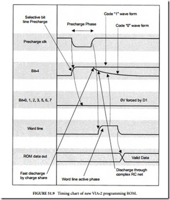
Figure 51.9 shows timing chart of each key signal and when Bit4 is accessed, for example, only this line will be precharged during precharge phase. However, all other bit lines are pulled down to GND by Dl transistors as shown in Figure 51.4. When VIA-2 code exists like N4 and Bit4, this line will be discharged. But if it does not exist, this line will stay at VDD level dynamically as described during word line active phase, which is shown in Figure 51.9. After this operation, valid data appears on data out node of data latch circuits [5].
In order to evaluate worst case speed, no VIA-2 coding on horizontal bit cell was used since transistor series resistance at active mode will be maximum with respect to GND. However, in this situation, charge sharing effects and lower transistor resistance during the word line active mode allow fast discharge of bit lines despite the increased parasitic capacitance on bit line to 1.9 times. This is because
all other nodes (N0–N7) will stay at GND dynamically. The capacitance ratio between bit line (Cb) and all nodes except N4 (Cn) was about 20:1. Fast voltage drop could be obtained by charge sharing at the initial stage of bit line discharging. About five voltage drop could be obtained on 8KW configuration through the charge-sharing path shown in Figure 51.8c. With this phenomenon, the full level discharging was mainly determined by complex transistor RC network connected to GND as shown in Figure 51.8a. This new ROM has much wider transistor width than conventional ROMs and much smaller speed degradation due to process deviations, because conventional ROMs typically use the minimum allowable transistor size to achieve higher density and are more sensitive due to process variations [5].
Comparison of ROM Performance
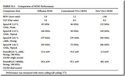
The performance comparison of each type of ROM are listed in Table 51.1. 8KW ROM module area ratio was indicated using same array configuration, and peripheral circuits with layout optimization to achieve fair comparison. The conventional VIA-2 ROM was 20% bigger than diffusion ROM, but new VIA-2 ROM was only 4% bigger. TAT ratio (days for processing) was reduced to 0.2 due to final stage of process steps. SPICE simulations were performed to evaluate each ROM performance considering low voltage applications. The DSP targets 2.5 V and 2.0 V supply voltage as chip specification with low voltage comer at 2.3 V and 1.8 V, respectively. However, a lower voltage was used in SPICE simulations for speed evaluation to account for the expected 7.5 supply voltage reduction due to the IR drop from the external supply voltage on the DSP chip. Based on this assumption, VDD = 2.13 V and VDD = 1.66 V were used for speed evaluation. The speed of new VIA-2 ROM was optimized at 1.66 V to get over 100 MHz and demonstrated 106 MHz operation at VDD = 1.66 V, 125dc, (based on typical process models). Additionally, 149 MHz at VDD = 2.13 V, 125dc was demonstrated with the typical model and 123 MHz using the slow model. This is a relatively small deviation induced by changes in process parameters such as width reduction of the transistors. By using the fast model, operation at 294 MHz was demonstrated without any timing problems. This means the new ROM has very high productivity with even three sigma of process deviation and wide range of voltages and temperatures [5].


Comments
Post a Comment