ROM/PROM/EPROM:ROM
Introduction
Read-only memory (ROM) is the densest form of semiconductor memory, which is used for the applications such as video game software, laser printer fonts, dictionary data in word processors, and sound-source data in electronic musical instruments.
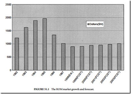
The ROM market segment grew well through the first half of the 1990s, closely coinciding with a jump in personal computer (PC) sales and other consumer-oriented electronic systems, as shown in Figure 51.1 [1]. Because a very large ROM application base (video games) moved toward compact disc ROM-based systems (CD-ROM), the ROM market segment declined. However, greater functionality memory products have become relatively cost-competitive with ROM. It is believed that the ROM market will continue to grow moderately through the year 2003.
ROM
Read-only memories (ROMs) consist of an array of core cells whose contents or state is preprogrammed by using the presence or absence of a single transistor as the storage mechanism during the fabrication process. The contents of the memory are therefore maintained indefinitely regardless of the previous history of the device and/or the previous state of the power supply.
Core Cells
A binary core cell stores binary information through the presence or absence of a single transistor at the intersection of the wordline and bitline. ROM core cells can be connected in two possible ways: a parallel NOR array of cells or a series NAND array of cells each requiring one transistor per storage cell. In this case, either connecting or disconnecting the drain connection from the bitline programs the ROM cell.
The NOR array is larger as there is potentially one drain contact per transistor (or per cell) made to each bitline. Potentially, the NOR array is faster as there are no serially connected transistors as in the NAND array approach. However, the NAND array is much more compact as no contacts are required within the array itself. However, the serially connected pull-down transistors that comprise the bitline are potentially very slow [2].
Encoding multiple-valued data in the memory array involves a one-to-one mapping of logic value to transistor characteristics at each memory location and can be implemented in two ways:
(i) adjust the width-to-length (W/L) ratios of the transistors in the core cells of the memory array; or (ii) adjust the threshold voltage of the transistors in the core cells of the memory array [3].
The first technique works on the principle that W/L ratio of a transistor determines the amount of current that can flow through the device (i.e., the transconductance). This current can be measured to determine the size of the device at the selected location and hence the logic value stored at this location. In order to store 2 bits per cell, one would use one of four discrete transistor sizes. Intel Corp. used this technique in the early 1980s to implement high-density look-up tables in its i8087 math co-processor. Motorola Inc. also introduced a four-state ROM cell with an unusual transistor geometry that had variable W/L devices. The conceptual electrical schematic of the memory cell along with the surrounding peripheral circuitry is shown in Figure 51.2 [2].
Peripheral Circuitry
The four states in a two-bit per cell ROM are four distinct current levels. There are two primary techniques to determine which of the four possible current levels an addressed cell generates. One technique compares the current generated by a selected memory cell against three reference cells using three separate sense amplifiers. The reference cells are transistors with W/L ratios that fall in between the four possible standard transistor sizes found in the memory array as illustrated in Figure 51.3 [2].
The approach is essentially a two-bit flash analog-to-digital (A/D) converter. An alternate method for reading a two-bit per cell device is to compute the time it takes for a linearly rising voltage to match the output voltage of the cell. This time interval then can be mapped to the equivalent two-bit binary code corresponding the memory contents.
Architecture
Constructing large ROMs with fast access times requires the memory array to be divided into smaller memory banks. This gives rise to the concept of divided wordlines and divided bitlines that reduces the capacitance of these structures allowing for faster signal dynamics. Typically, memory blocks would be no larger than 256 rows by 256 columns. In order to quantitatively compare the area advantage of the multiple-valued approach, one can calculate the area per bit of a two-bit per cell ROM divided by the area per bit of a one-bit per cell ROM. Ideally, one would expect this ratio to be 0.5. In the case of a practical two-bit per cell ROM [4], the ratio is 0.6 since the cell is larger than a regular ROM cell in order to accommodate any one of the four possible size transistors. ROM density in the Mb capacity range is in general very comparable to that of DRAM density despite the differences in fabrication technology [2].
In user-programmable or field-programmable ROMs, the customer can program the contents of the memory array by blowing selected fuses (i.e., physically altering them) on the silicon substrate. This allows for a “one-time” customization after the ICs have been fabricated. The quest for a memory that is nonvolatile and electrically alterable has led to the development of EPROMs, EEPROMs, and flash memories [2].


Comments
Post a Comment