Field-Programmable Gate Arrays:Various Field-Programmable Gate Arrays
Various Field-Programmable Gate Arrays
FPGAs have different basic structures, as already discussed. If we look at their details beyond this, there are different types of FPGAs, as follows.
FPGAs Based on SRAMs
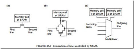
FPGAs based on SRAMs connect lines by controlling a pass transistor, a transmission gate, or a multiplexer, each of which is controlled by a flip-flop (i.e., one memory cell of SRAM) as shown in Figure 47.5. Any horizontal line and a vertical line shown in Figure 47.1 can be connected at some of their cross points (shown with dots in Figure 47.1). Suppose a flip-flop is used. If the flip-flop is on, these two connection lines are connected; if it is off, they are not. By connecting horizontal connection lines and vertical connection lines at appropriate cross points in this manner, the outputs of one logic block can be connected to the inputs of other blocks.
FPGAs based on SRAMs are available from Xilinx, Atmel (previously Concurrent Logic), and others. Lines are connected by transfer gates (or pass transistors) in Figure 47.5(a), transmission gates in (b), or multiplexers in (c) that are controlled by ON or OFF states of memory cells of SRAM. A multiplexer is typically used to connect one of several incoming lines to one outgoing line.
FPGAs based on SRAMs were started by Xilinx [6,10]. Many logic blocks that contain SRAMs and flip-flops are provided in FPGAs of this type, along with many pre-laid connection lines, as illustrated in Figure 47.1. Each block is connected to nearby one-line segments, as shown in Figure 47.6. A switch matrix shown with a square is a set of multiplexers, where any one outgoing line segment can be connected to any of many incoming line segments. Besides these one-line segments, where by connecting many of them through switch matrices, long lines can be formed, there are global long lines that can be formed by connecting fewer segments, each of which has longer segment length. (Note that a long line formed by connecting many one-line segments has a long delay because delays of many switch matrices are added to the delay of the lines due to parasitic capacitance.) In this sense, delay times on lines that consist of many line segments are unpredictable. Each logic block consists of a RAM along with several flip-flops, as shown in Figure 47.7. Xilinx calls logic blocks configurable logic blocks (CLBs). Users can store logic functions in these SRAMs and connect the blocks by lines as they want.
Each CLB packs a pair of flip-flops and two independent four-input function generators, as illustrated in Figure 47.7. The two function generators whose outputs are labeled F′ and G′ are realized with RAMs and are each capable of realizing any logic function of their four inputs, offering designers
sufficient flexibility, because most combinational logic functions does not need more than four inputs. Thirteen CLB inputs provide access to the function generators and flip-flops. These inputs and four CLB outputs connect to the programmable interconnect resources outside the block. Four independent inputs, F1–F4 or G1–G4, are provided to each of the two function generators. The function generators are used as look-up table memories; therefore, the propagation delay is independent of the function being realized. A third function generator, labeled H′, can realize any logic function of its three inputs, F′ and G′, and a third input from outside the block (H1). Signals from the function generators can exit the CLB on two outputs; in other words, F′ or H′ can be connected to the X output, and G′ or H′ can be connected to the Y output. Thus, a CLB can realize any two independent functions of up to four variables, or any single function of five variables, or any function of four variables together with some functions of five variables, or it can even realize some functions of up to nine variables. Realizing a variety of functions in a single logic block reduces both the number of blocks required and the delay in the signal path, thus increasing both density and speed.
The CLB contains also edge-triggered D-type flip-flops with common clock (K) and clock enable (EC) inputs. A third common input (S/R) can be programmed as either an asynchronous set- or reset-signal independently for each of the two flip-flops; this input can also be disabled for either flip-flop. Each flip- flop can be triggered on either the rising or falling clock edge. The source of a flip-flop data input is programmable; it is driven either by the functions F′, G′, and H′, or the Direct In (DIN) block input. The flip-flops drive the CLB outputs, XQ and YQ.
In addition, each CLB function generator, F′ or G′, contains dedicated arithmetic/logic unit (not shown in Figure 47.7) for the fast generation of carry and borrow signals, greatly increasing the efficiency and performance of adders, subtracters, accumulators, comparators, and counters. Multiplexers in the CLB map the four control inputs, labeled C1 through C4 in Figure 47.7, into the four internal control signals (H1, DIN, S/R, and EC) in any arbitrary manner.
This FPGA has the following advantages:
• Once logic design is finished, logic functions can be realized by this FPGA in minutes by writing design information into SRAMs and flip-flops, as necessary.
• Quick realization of complex logic functions that require a large number of logic gates and therefore cannot be realized with FPLAs or PALs is the great advantage of this type of FPGA.
The disadvantages include the following:
• If the power supply to this FPGA is turned off, the information is lost and, consequently, design information must be written each time the power supply is turned on.
• Also, compared with mask-programmable gate arrays, its chip size is roughly 10 times larger and its speed is far slower. But its speed is still much faster than software run on a general-purpose computer.
If the number of CLBs is to be minimized, this type of FPGA presents a totally new type of logic design problem and there is no good design algorithm known. Traditional logic design problems are realization of given functions with a minimum number of simple logic gates of certain types (e.g., NOR gates or negative gates). But with this type of FPGA, we have to realize the given functions with logic functions that can fit in the SRAMs provided, where these functions can be far more complex than the NOR functions or negative functions that logic gates represent. But the number of CLBs is not necessarily to be minimized because after debugging logic design, final logic networks to be manufactured in large volume are usually realized with logic gates but without RAMs.
Using FPGAs of this type, the development time of mask-programmable gate arrays that are completely verified can be often shortened to less than half, and new computers can be introduced into the market quickly. In other words, when logic design is finished, computers can be shipped immediately in FPGAs to major customers for testing. After these customers find bugs, the designers fix them and the production of mask-programmable gate arrays can be started. Without FPGAs, the computers have to be shipped to customers for testing after manufacturing mask-programmable gate arrays—which takes several weeks. Then, when the customers find bugs, the designers start the production of the second mask-programmable gate arrays. Thus, when mask-programmable gate arrays are used, a new gate array must be manufactured, spending a few weeks, for each correction of bugs and testing by customers. The completion of the computer will be significantly delayed and with far greater expense. If the design is complex, the designers need repetition of tests by the customers. In contrast to this, if FPGAs are used, the designers can send the debugged design to the customers online, and customers can start the second test instantly by revising the contents of the FPGAs.
Atmel’s FPGA uses SRAMs, but logic blocks and architecture are similar to Actel’s, unlike Xilinx’s whose logic blocks contain SRAMs which are used as look-up tables. FPGAs of Plessey are based on SRAMs, but the architecture looks like the sea-of-gate array shown in Figure 47.2. Altera also has FPGAs based on SRAMs, using the architecture with non-volatile memory [10]. FPGAs of Algotronix use SRAMs, but logic blocks are mostly multiplexers. AT&T Microelectronics also has FPGAs based on SRAMs similar to Xilinx’s.
FPGAs Based on ROMs with Anti-Fuses
There are FPGAs based on ROMs that are programmable with anti-fuses. These FPGAs are available from Actel, QuickLogic, and Crosspoint Solutions. Connection of lines in this type of FPGA can be made by the use of anti-fuses. Once an anti-fuse becomes conductive, it cannot be non-conductive again, unlike FPGAs based on SRAMs. Typical applications utilizing 85% of the available logic gates, however, need to use only 2 to 3% of these anti-fuses (i.e., to be changed to conductive state). Note that if fuses, instead of antifuses, are used, 97% or 98% of fuses need to be disconnected, requiring disconnection of a huge number of fuses.
Actel’s FPGAs are of row-based structure, as illustrated in Figure 47.3 [3–5,10]. The actual logic block array of Actel is shown in Figure 47.8. A logic block (Actel calls it a logic module) for a simple model of Actel’s FPGA consists of three multiplexers and one OR gate, as shown in Figure 47.9, where some of their inputs and outputs can be complemented. This logic module, which has eight inputs and a single output, can realize many different logic gates with some inputs inverted, as follows: four basic logic gates
(i.e., NAND, AND, OR, and NOR gates with 2, 3, or 4 inputs); EXCLUSIVE-OR gates, EXCLUSIVE-OR- OR gates, EXCLUSIVE-OR-AND gates, OR-EXCLUSIVE-OR gates, AND-EXCLUSIVE-OR gates, AND-
OR gates, and OR-AND gates; and a variety of D latches. Other models of Actel have more complex logic modules that contain latches.
FPGAs Based on Non-Volatile Memories
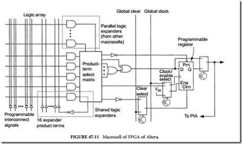
Altera has FPGAs that are based on non-volatile memory for connecting lines [10]. This FPGA has bus- based structure illustrated in Figure 47.10 (i.e., Figure 47.4). The inputs and outputs of each logic block can be connected to bus lines, as shown in Figure 47.10. Altera calls these bus lines PIA (Programmable Interconnect Array). Altera claims that delay times on PIAs are more predictable than those on lines that consist of many line segments. A logic block contains of 16 logic macrocells, such as the one shown in Figure 47.11.
FPGAs of Advanced Micro Devices and Lattice Semiconductor Corp. are based on a different type of non-volatile memory, using PALs as logic blocks that can be connected with switch matrixes similar to Altera’s.


Comments
Post a Comment