LAYOUT CONSIDERATIONS DUE TO PROCESS CONSTRAINTS:WIDE METAL SLITS
WIDE METAL SLITS
Power supply lines in a chip are designed to be very wide so that electromigration and resistance effects are minimized. Are there maximum limits to the width of metal lines? In general the answer is no. However, there is one problem with very wide metal lines that occurs when the temperature of the chip rises high enough to cause the metal to expand significantly.
Figure 8.1 shows the effect of heat on the metal as it expands. As the metal heats up, the sideways inertia of a large piece of metal prevents sideways expansion. As a result the expansion of the metal is in the center. This causes the center areas of the metal to expand upwards. This effect is not as significant for smaller signals, as the upward expansion of the metal occurs with a smaller force because of the smaller size and lower sideways inertia.
If the metal expands repeatedly with enough force, the metal will eventually crack the isolation and passivation layer that protect the wafer. Impurities and particles will work their way onto the chip, react with the different materials, and cause the chip to fail or work unreliably.
To address this problem, layout designers are required to put slits or holes in the metal at regular intervals. This technique has the effect of reducing a very wide metal to one that has many smaller areas that happen to be connected together.
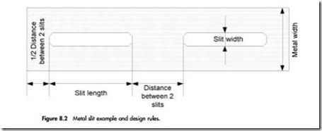
Figure 8.2 shows an example of a metal line with metal slits cut out of it. The design rules for slits are very process dependent because they depend on the metal granularity, temperatures of expansion, type of material, etc.
Note the following:
• Slits have 45-degree corners to alleviate stress induced by high current densities within the metal.
• A general guideline for the maximum size of line that does not require a slit is 35 mm.
• Divide extra very wide metals into increments that are lower than the maximum allowed width. (For example, if the maximum metal width without slits is 50 mm and we are inserting slits into a 100-mm line, then it is advisable to use two slits in the line instead of one.)
• It is easiest to insert slits into a wide metal line by building a structurally correct unit cell and instantiating it as required.
• Slits should always be implemented in the direction of current flow. This is especially important for T junctions or other configurations.
• Slits generally can be implemented over a range of lengths. Try to use an average size so the slits can be easily adapted for special area such as corners and junctions.
• Discount the effective metal width of the line by the width of the slit or similarly add to the desired width of the line the width of a slit to account for the lost area. For example, if a metal line is desired to be 100 mm wide, two slits are to be inserted, and the slit width is 5 mm, then the total width of the line will consume 110 mm of space.
• Analyze the current flow before you make slits in corners, T-junctions, and power pads.
• If the DRC cannot check all of the cases presented here, a visual inspection is necessary.
Design rules for the definition of slits are usually well described, but in many cases the conditions under which they are to be used are not. Specific areas where slits should be used are for power lines near the corners of the chip and the case of a pad connection in a T shape to a wide metal bus.
Figure 8.3 shows a corner power track and the way the design rules are to be respected in this case.
As we can see in Figure 8.3, it is important to have a small bridge of metal during the 45-degree turn to increase metal physical resistance against chip corner breakage during cut and package assembly. Figure 8.4 shows a proper connection from a power pad to an internal bus with correct metal slits. The current flow is shown as a guide for understanding the implementation of the slits.


Comments
Post a Comment