LAYOUT DESIGN TECHNIQUES TO ADDRESS ELECTRICAL CHARACTERISTICS:CAPACITANCE
CAPACITANCE
The definition and sources of capacitance are important concepts for a layout designer to understand. In some special cases the circuit schematic requires capacitance, but in general the emphasis in optimizing a layout design is to minimize the parasitic capacitance inherent to the different layout structures.
Capacitance affects several different characteristics of a design. When two equivalent designs are compared, the design with the higher capacitance will have a resulting increase in all of the following:
• Signal delay
• Power consumption
• Coupling effects to and from neighboring structures
A review of the definition of capacitance will give us an unders- tanding which good design practices reduce capacitance for various layout design styles.
The general formula for the calculation of the capacitance of a conductor is where A is the surface area of the specific conductor, d is the physical distance between the conductor and the reference node, and e is a constant representing the characteristics of the insulating layer between the conductor and the reference node. Figure 7.9 shows the theoretical definition of a capacitor.
From this formula it should be apparent that there are two ways to mini- mize the capacitance of a signal (e is a characteristic of the manufacturing process and is not within the layout designer’s control):
1. Reduce the area of the capacitor—this means reducing the overlapping regions of the two “plates” or polygons
2. Increase the distance between the plates of the capacitor
The effect of a capacitance C on a signal is to limit the rate of change in voltage (dV/dt) on the line by requiring more charge or current I according to the formula t is from this relationship that we derive the delay formula tdelay = RC.
Designing Capacitors
As we mentioned, there are certain cases where a capacitor is an integral part of the circuit design. Examples include the following:
• DRAM memory cell
• Power supply decoupling capacitors
• Power supply generator reservoir capacitors
• Delay chains
• Specialized analog circuits such as switched capacitor applications
How can capacitors be predictably designed?
As described in Chapter 5, a DRAM memory cell capacitor is simply
the overlap of two layers that has been optimized to be very close together. In this case the d distance term has been minimized to increase the capacitance value.
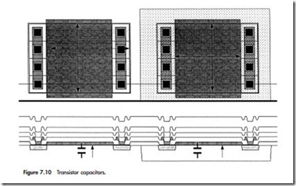
Within a standard CMOS process, the choice of layers to implement an effective capacitor is really limited to one case. By design, a transistor is manufactured to have a very small distance d between the gate poly and active layers. The source and drain nodes connect to one terminal of the capacitor and the gate node is the other.
Figure 7.10 illustrates two implementations of an NMOS transistor-based capacitor. One is in the substrate and the other has been drawn within an N-well.
The N-well transistor results in a higher effective capacitance because of the lower threshold upon which the transistor starts to operate.
Power supply decoupling capacitors may be the most common use of intentional capacitors, so a few comments about them are warranted. These capacitors are connected between two power supply nodes (such as VDD and VSS) to “decouple” the two nodes and provide dynamic charge to what can be very noisy signals. This decoupling serves to stabilize the power supply voltage and increases the reliability of the chip operation.
In order to provide a measurable amount of charge, these capacitors need to be pervasive on the chip, and the effective size of the total capacitance can be in the nF or nanoFarad range. Some planning is required to achieve an effective implementation; however, power supply lines are generally readily available in many places, so it is not too difficult to find space once the regular circuitry has been implemented. It is also recommended to isolate these large transistors with guard rings to avoid noise coupling to unwanted circuitry.
Minimizing Parasitic Transistor Capacitance
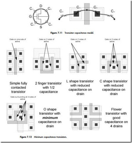
There are many parasitic capacitances inherent in a transistor, as shown in Figure 7.11.
Figure 7.12 shows a few examples of transistors designs that significantly reduce the capacitance of the drain CDB. Comments for the figure are given in Table 7.2.
In general, if minimum design rules are used, then the transistor capacitance can be optimized using the techniques shown in Figure 7.12.
Interconnect Capacitance
Parasitic interconnect capacitance is impossible to avoid, and in most cases it is an effect that must be dealt with by compensating for the load by proper circuit design.
It is mainly for the modeling and calculation of the interconnect capacitance for every node in a design that extraction tools are used. This section will present the concepts behind the sources of capacitance that the extraction tools try to model and calculate.
Consider that a chip is manufactured from many layers placed on top of one another. The bodies near a particular polygon are numerous, and each pair of near bodies creates a parasitic capacitor. These days it is recognized that 70 to 80 percent of the total capacitance of any particular node is due to the parasitic capacitance of the interconnect routing. The shift toward dealing with interconnect loading rather than transistor loading has come about as a result of increased die sizes, increased number of interconnect layers, and smaller line pitches.
Once an understanding of the source of interconnect capacitance is reached, then it is a matter of addressing this issue using advanced techniques. Figure 7.13 gives a three-dimensional view of various scenarios to illustrate the different sources of interconnect capacitance.
One presentation on the CD-ROM shows an example of extraction that is trying to bring the real data back to the circuit design.
The capacitance of any signal is fundamentally composed of three types of elements, as shown in the Single Line Capacitance Model portion of Figure 7.13:
1. Parallel-plate capacitance: This is the simple capacitance model that was described in the beginning of Section 7.2.
2. Fringe capacitance: This capacitance is caused by the electric field induced as current flows down the line.
The modeling and calculation of this capacitance is well beyond the scope of this book but it is important to know that the fringe capacitance can be a very high proportion (~50 percent) of the total interconnect capacitance!
Suffice it to say that the fringe capacitance is dependent on the distance d of the signal from the body in question.
It is only recently that extraction tools have been developed to address this issue, as they historically have been limited to parallel plate capacitance type of models.
3. Coupling capacitance: Coupling capacitance is defined as a capacitance from one signal node to another.
A simplistic model to visualize the coupling capacitance would be to use the parallel-plate and fringe capacitance calculation between the signals in question.
The Coupling Capacitances portion of Figure 7.13 tries to illustrate this point. Near-body capacitance can be to other signals or to a variety of structures such as power supply nodes and the substrate, as shown in the figure.
Accurate modeling of coupling capacitance is limited to very specific applications simply because the tools and methodologies behind simulating and
extracting the size of networks that would take into account all near-body capacitance are not practical.
It is simplistic to assume that the capacitance of a node is always relative to ground. Considering coupling capacitance is crucial in the scenario where the two signals on either side of the capacitor are changing voltage in the opposite direction at the same time. This scenario is shown in Figure 7.14.
In this case the effect of the coupling capacitance to the delay of the signal is double that of the case where the reference node is a static signal. The driver of the line is trying to drive the signal one way and is fighting the parasitic capacitance of the line. As the reference node voltage of the capacitor is changing in the opposite direction, it couples into the line and the effect is to delay the signal even more.
Conversely, if two signals are being driven in the same direction, then they help each other.
Now that we understand the sources of parasitic capacitance, what are some techniques to reduce the different capacitive loads on a given signal?
• Reduce the area of the parallel plates.
What does this mean in a layout sense? Either shortening the length of the signal or minimizing the width, or both.
It is important to note that in the case where a signal is simply reduced in width by 50 percent, the capacitance is reduced only by 25 percent because the parallel plate portion of the line is 50 percent of the total and, without changing the length, the fringe term remains constant.
In contrast, shortening the length of a given signal by 50 percent will result in 50 percent capacitance savings because both the parallel plate and fringe terms are affected equally.
• Reduce the distance d or dielectric distance between the parallel plates.
Again, what does this mean in a layout sense? Whenever possible, route critical signal lines in empty channels and minimize the amount of area that the signal is routed over or under other layers.
As an example, assuming an empty routing channel was used, using the topmost routing layer would have the least capacitance relative to the substrate terminal when compared to other layers.
An implementation using the top routing layer and appearing as close to the Single Line Capacitance model shown in Figure 7.13 is the ideal to shoot for.
• Increase the spacing between signals on the same layer to address the coupling capacitance between them. We call this signal spreading, and it is exceptionally useful in areas where the routing congestion is low. Please review the Sagantec presentation on the CD-ROM.
• In the case of differential signals, implement a “twisting” scheme that reduces the coupling effects of the adjacent lines by ensuring that any coupling affects both signals of the pair equally. Figure 7.15 demonstrates this concept for signal XX and introduces the concept of shielding.
• Shield critical signals with a signal that remains at a static level. This technique eliminates the possibility of the worse-case coupling scenario illustrated in Figure 7.14.
The concept of shielding signals was imported from the printed circuit board (PCB), where some signals that are supposed to provide the circuits with a reference voltage are isolated from interference to a greater extent than other signals. One example of shielding is shown in Figure 7.15, but there are more elaborate techniques. A signal can be shielded on both sides, as shown in Figure 7.16. In this case we are isolating the signal from influences on the same layer.
Figures 7.17 and 7.18 show examples of shielding of greater sophistication in that the signal in question is completely surrounded, including in directions above and below the conductor. The capability of shielding is dependent on the available routing, as shown by the two figures.


Comments
Post a Comment