LAYOUT DESIGN TECHNIQUES TO ADDRESS ELECTRICAL CHARACTERISTICS:RESISTANCE
RESISTANCE
The convention in IC design for resistance calculation is to characterize each conductor layer in terms of resistance per “square.” One “square” is defined as the condition when the length of the conductor equals the width. The formula for calculating the resistance of a conductor is where r is the resistivity of the layer measured in W/D, l is the length, and w is the width of the conductor.
From this formula it should be apparent that there are two ways to minimize the resistance of a polygon (r is a characteristic of the manufacturing process and is not within the layout designer’s control):
1. Reduce the length of the polygon
2. Increase the width of the polygon
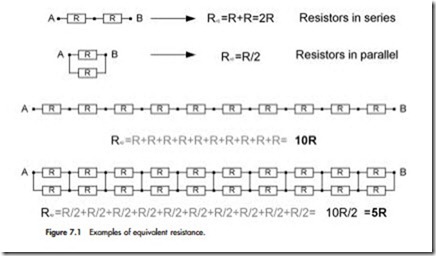
A review of the calculation of equivalent resistance for resistors connected in series and in parallel is important to understand when good design practices reduce resistance for various layout design styles.
Figure 7.1 shows different examples of resistors connected in different ways and a calculation of the total resistance between the two nodes, A and B. It is important to note that resistors in series are accumulative and resistors in parallel reduce the effective resistance.
Minimizing Resistance in Transistor Design
We have already discussed resistance in terms of routing in Chapter 6. Now, let’s consider the resistive effects in transistor-level layout design.
Remember that a transistor in CMOS is made of source (active), gate (poly- silicon), and drain (active) regions, but to make it work we need signals connected to all three terminals. Thus, contacts to the source and drain are important to consider.
Figure 7.2 shows a fairly complex resistance model of the transistor with different resistors representing the many different current paths across the width of the transistor. Every current arc that is shown in the polygon layout is represented in the resistance model. The legend gives approximate numbers for each type of resistance and demonstrates the relative values of each of the resistors in the circuit. These numbers would be representative of a 0.25-mm process.
It is interesting to note that the active resistance is dominant and is 1,000¥ more resistive than metal1 and more than 10¥ more resistive than a metal1 contact. These numbers give us a good starting point for minimizing the overall resistance from the two metal lines: try to minimize the active resistance!
Figure 7.3 shows the effect of different contacting schemes for a transistor design to illustrate this concept.
All of these examples consider the contact resistance in the analysis. Remember that the contacts are three-dimensional columns of metal or poly, and they add to the resistance of paths. The number of contacts in any connection is important to consider, because for each contact the resistance is reduced by introducing another parallel current path from the conductor. This is especially important for high current carrying signals such as clocks and power supplies.
The choice of layout style or number of contacts for transistor should be made with the application and the priority of the characteristics in mind.
For example, analog, high-speed, RF, and DRAM circuits are only a few applications that rate performance and reliability highly, so fully contacted transistors are the norm. If routability is a key issue, then using the transistor layout shown in case 2 may be appropriate. In certain places, the higher resistance exhibited in case 2 may not have an adverse effect; therefore, the benefit of routability makes this option attractive.
We would like to remind you that the calculated values should be used relative to each other, and they serve to help us evaluate the differences between these types of connections.
The transistor shown in Figure 7.4 is an extreme example that demonstrates a solution to a layout design problem where performance is sacrificed for routability. There are cases where this layout is appropriate. Certain processes will have significantly different characteristics in terms of the resistivity of the layers. For example, there are processes where the active layer is metallized and has a much lower (1/10) resisitivity than our example. In this case the performance of the transistor may be acceptable and we can take advantage of the routing channels to optimize the cell layout. These processes are more costly, but we should always be on the lookout to take advantage of special characteristics for layout design.
Controlling resistance is an important concept for a layout designer to understand. In some cases an intentional resistor may be needed.
Resistors are required for the following:
• Voltage dividers
• Delay elements
• Dynamic logic loads
• SRAM cells
• ESD input protection structures
• Many analog circuit applications
In all of these cases we want a resistor and an accurate one as well.
The first step in implementing any resistor is to choose the appropriate layer.
An appropriate choice of layer is possible by considering the following factors:
• Resistivity of the different layers
• Variation in resistivity under different process and environmental conditions (temperature)
• Variation in layer width under different process conditions
• Resulting area of resistor given chosen layer In most cases gate poly is chosen as the resistor material, as its resistance is relatively high, the resistivity and width are tightly controlled, and the resulting area is not prohibitive. Some processes have a special highly resistive layer that is ideal for this application.
Resistance is calculated using squares, so to implement a specific resistance value a constant width is selected and the length of the polygon can be calculated by rearranging the formula
Wider polygons result in a longer path for a specific resistance, so the width should be chosen that produces a resistor of reasonable size. Minimum design rule polygons are usually avoided because the variation in width is most acute under this condition. It is also a good idea to standardize on a resistor polygon width for an entire chip so that all resistors will vary equally over the die. Remember to consider the effect of contact resistance!
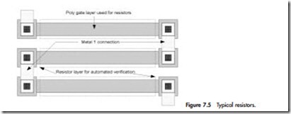
Figure 7.5 shows examples of typical poly resistors. They are made of poly gate, connected to signals through contacts, and defined by a special resistor layer. This layer is used only for documentation and LVS purposes. It identifies the region where a resistor is recognized to establish the device for layout verification. CAD tools require that the contact layer does not overlay this resistor identification layer.
Note that resistors are prime candidates for metal options, as they are typically used in analog circuits that frequently require fine-tuning.
We can see from Figure 7.6 that these are more area efficient solutions, as they sometimes have to fit in the areas of transistors without using too much space. The disadvantage of such resistors is that the resistance is not easily calculated because of the corners in the poly layer. As a best approximation, we can use the centerline of the poly divided by the width to calculate the total resistance of the line.
In analog or RF layout designs, we may have to shield the resistor fingers from itself to avoid coupling. Figure 7.7 shows an example of such a resistor.
In some very sensitive circuits when there are two resistors connected to signals that are switching on opposite clock edges, we can balance the coupling effects between the two resistors to ensure that they both operate in a similar manner. These are referred to as balanced interlaced resistors. An example is shown in Figure 7.8.


Comments
Post a Comment