Practical considerations , Transistor-transistor logic (TTL) and Digital-to-analog converters (DACs).
Practical considerations
Design of any logical system needs care. Practical points that need consideration are speed, noise and power consumption.
Speed of a logic gate is defined as the propagation delay; this is the time a signal takes to travel from the input of a logical unit to the output, shown in (a). Allied with this is the rise time, defined roughly as the time taken for a signal to travel from one state to another, shown in (b). these two factors determine the maximum speed at which the system can operate. Normal 'cooking' logic can operate up to around 5 MHz and high speed logic can operate at 50 MHz.
Noise is often a major problem, particularly in industrial systems. Noise causes memories to set, monostables to trigger and counters to count. Broadly speaking there are four classes of noise:
(I) pick-up signal inputs
(2) supply-borne externally generated
(3) supply-borne internally generated
(4) cross-talk and reflections.
Pick-up on signal inputs can be avoided by avoiding cable runs shared with high current cables and the use of opto-isolators on all inputs and outputs. Cables should be screened and the screen earthed at one end only to avoid earth loops.
External supply noise is caused by the switching of heavy loads. It can be avoided by the use of mains filter and constant voltage transformers. In extreme cases, the logic can 'float' on a battery which is charged from the mains.
Internal supply noise is quite a common problem. As gates switch, their load current changes very quickly, and the di/dt, combined with the inductance of the supply leads, causes voltage spikes. TIL (see next section) is particularly notorious for this effect. The cure is to adopt a sensible supply layout and to liberally decouple the supply with 0.0I J.1F capacitors on every other integrated circuit package.
Cross-talk and reflections have a common cause. Logic signals have fast edges, and line lengths over a few hundred centimetres need to be treated as transmission lines. There are special line driver gates and receivers available, and their use should be considered for lengths of over a few metres. Cross-talk can be minimised by avoiding lengthy parallel tracks.
Logic families have their noise immunity defined in their data sheets. Somewhat simplified, it is the disturbance that has to be added to a logical state before the signal might be detected as a signal of the opposite state under the worst conditions of supply and load.
Digital systems operate at high speed, and to do this some logic families use low value resistances internally to minimise the effects of stray capacitance. This tends to lead to quite high supply currents. Large logic systems using tens of amps at 5 V are by no means uncommon. Supply layout obviously needs care in the design to avoid voltage drops, and adequate protection should be given to harness wiring to ensure that faults do not lead to overheating of cables.
Gate outputs and inputs cannot be connected together indefinitely, and loading of each output must be considered. An output has a defined fan-out, which is the number of standard gate inputs it can drive (typically I 0 for TTL and 50 for CMOS).
Inputs have a defined load (called the fan-in) which relates to the number of equivalent gate inputs. Most simple inputs have a fan-in of I, but some complex clock inputs on microprocessor integrated circuitscan have fan-ins of 2 or 3. To ensure correct operation the sum of all the fan-ins connected to a gate output must be less than or equal to its fan-out capability.
Transistor-transistor logic (TTL)
TTL utilises a single 5 volt supply and is based on the NAND gate element in (a). The rather odd-looking dual-emitter transistor can, for analytical purposes, be considered as two transistors in parallel, as in (b).
The two output transistors are known as a totem pole output and serve to increase gate speed. Transistor TR4 acts as a saturated transistor with a low impedance output while transistor TR3 acts as an emitter follower. Logic states are well defined (3.5 V for I, 0 V for 0) and low output impedance in both states makes edge speeds relatively independent of load.
Totem pole output does, however, bring a few problems. As the output changes state, both transistors conduct together for a short time. This causes a brief large current pulse to be drawn from the supply. This can be as high as I 00 rnA, and can be a source of noise
problems. Frequent decoupling of the supply rails with 0.01 J.lF
capacitors is necessary.
TTL uses saturating transistors to define the logic levels, and as such suffers from a phenomenon called charge storage. This causes a saturated transistor to hold on for a few nanoseconds when it is turned off. Hole storage can be overcome by the inclusion of a Schottky diode, as in (c), to prevent the transistor saturating.
There are three common TTL families. These differ in speed and power requirements (which is always a trade-off that needs to be made in digital circuits. Low impedances give fast speeds but high power consumption).
Other less common variations are high speed (now really defunct, as it is slower than Schottky), low power and advanced Schottky.
TTL logic is almost universally based on the Texas Instruments 74-series range, with device numbering of the form 74suffixNNN, where NNN defines the function (e.g. 74LS123).
TTL was once the most widely used logic family, but its requirements for expensive high-current 5 volt power supplies have led to it being overtaken by the next logic family, CMOS.
Complementary metal oxide semiconductor logic (CMOS)
CMOS is almost the perfect logic family. It requires no special power supplies and can operate from a single rail anywhere in the range 3 to 15 volts. It uses little power when operated at low speeds (typically 0.01 mW per gate) and is adequately fast for most
applications (but not as fast as S-series TTL). CMOS gates have high input impedances and this allows very high fan-outs, typically around 50 compared to I 0 for TTL.
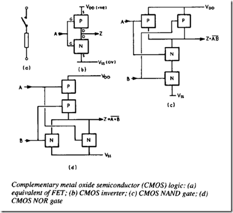
CMOS is built around the two types of field effect transistor described earlier. These can be considered as a perfect switch in series with a resistor, as in (a). It is thus a straightforward job to construct logic gates, the circuits for an inverter NAND and NOR gates being shown in (lrd).
A CMOS input is simply the gate of a FET, and has a very high impedance which, in early versions, allowed damage from high voltage static electricity during handling. More modem devices are well protected and can be handled almost like any other component.
It is, however, still good practice to handle CMOS on an earthed sheet and use earthed wrist straps when inserting or removing CMOS integrated circuits.
Although CMOS is a low-powered family, power consumption does rise with increasing speed as stray capacitance is charged and discharged. Above toggle speeds of about I MHz, CMOS and LS TTL have similar power consumption. In any system, however, all the gates are not toggling at the same speed, and a CMOS circuit will typically use one-tenth to one-quarter of the equivalent LS TTL circuit.
CMOS integrated circuits are based around the 4000-series, which is a rational combination of the RCA COSMOS range and the Motorola MeMOS. Devices are coded 4NNNsuffix (e.g. 4002B) where the suffix denotes a buffered (B) or unbuffered (A) device. B series should be used for all new designs. A 74C-series is available which is pin-compatible (but not electrically compatible) with 74- series TTL.
CMOS is well suited to the design of complex high density integrated circuits. Most microprocessor integrated circuits and their support chips, such as memories, are based on CMOS technology.
Emitter coupled logic (ECL)
ECL has the merit of being the fastest available logic family, with propagation delays as low as I ns and operating speeds up to 500 MHz. The two main constraints on operating speed of any digital circuit are charge storage and stray capacitance. ECL overcomes the first problem by using non-saturating transistors and the second by using low impedances. Both of these solutions result in high power consumption, typically over 30 mW per gate.
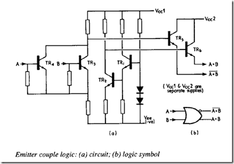
The circuit of an ECL OR/NOR gate is shown in (a). This has the logic symbol shown in (b). The circuit resembles a DC amplifier long-tail pair, with inputs A, B being compared with the reference voltage on transistor TR2 base. Emitter follower outputs are used to give good drive capability.
ECL is not easy to use. Its logic swing is small and poorly defined (-0.8 V and -1.6 V) so its noise immunity is poor. It needs three high current stable power supply rails. Its biggest problem, however, is inherent in its high speed. The very fast edges demand that interconnecting leads be dealt with as transmission lines, and hence much care must be put into the layout design. An ECL circuit cannot be thrown together; multilayer PCBs must be used.
Digital-to-analog converters (DACs)
An 8-bit binary number can represent a decimal number in the range 0 to 255. It can also represent a voltage in the range 0 to 2.55 volts if one bit is said to represent 10mV. Any other scaling could, of course, be chosen.
A device which converts a digital number to an analog voltage is called a digital-to-analog converter. Two common digital-to-analog circuits are shown.
First digital-to-analog converter (a) switches different resistor values to the input of an inverting op-amp from a fixed reference voltage. If switches D and B are closed, for example, the output voltage will be 1.25 times Vref·
Second digital-to-analog converter (b) is easier to construct in integrated circuit form as only two values of resistor are used, regardless of the number of bits. This circuit is known, for obvious reasons, as an R-2R ladder.
In both circuits CMOS transmission gates are used to perform the switching. Digital-to-analog converters are readily available in integrated circuit form, typical devices having a resolution of 12 bits (one part in 4096).
Analog-to-digital converters (ADCs)
An analog-to-digital converter converts an analog voltage to an equivalent digital representation for use by a computer or logic system. There are many different circuits, but most work by comparing the output of a logic-driven digital-to-analog converter with the input voltage.
The circuit shown is called a ramp analog-to-digital converter and is one of the slower, but simpler, circuits. A binary counter is connected to a digital-to-analog converter. As the counter counts up from zero, the digital-to-analog converter output is a ramp. This voltage is compared with the input voltage, and when the two are equal the counter is stopped. The count value is then a digital representation of the input voltage. The Q output of tl flip-flop indicates 'analog-to-digital converter busy' while the Q output indicates 'count complete'.
Analog-to-digital converters are, inevitably, most often used in integrated circuit form. Typical devices will give a 12-bit (one part in 4096) resolution. Conversion times of a few microseconds can be obtained with more refined circuits. The fastest analog-to-digital converters, called flash converters, are used to digitise television pictures for units which convert between different television standards and for television special effects units.
Optoelectronics
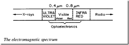
Light is an electromagnetic phenomenon, which exhibits many of the properties of radio waves. Visible light is the part of the electromag netic spectrum covering wavelengths from about 0.4 !lffi (violet) to 0.8 !liD (red) (400-800 nm). Optoelectronic devices cover a far wider range than this, from the ultraviolet into the infrared. The relevant parts of the spectrum are shown.
As there is a close family resemblance between optics and electronics, it is not surprising that the multi-disciplinary topic of optoelectronics has become increasingly important in recent years. Optoelectronic devices fall into three categories: ( 1) devices that respond to light (sensors); (2) devices that emit light (emitters); (3) devices that utilise light.


Comments
Post a Comment