Karnaugh maps , Storage and D-type flip-flop.
Karnaugh maps
A Karnaugh map is an alternative way of representing a truth table -in the form of a two-dimensional grid. Two-, three- and four variable maps are shown. Each square on the table represents one line of a truth table. For example:
The axes on a Karnaugh map are labelled so that a move between adjacent squares vertically and horizontally results in the change of only one variable. For example, the map below represents the four lines of a truth table:
The map, however, reveals that both B and D can change without affecting the output. The marked squares in fact represent A.C so the above Boolean expression simplifies to:
Z = A.C
The rules for minimising an expression with a Karnaugh map are simple:
(a) Plot the expression on the map either from a Boolean equation or truth table
(b) Form new groups of Is. Groups must be rectangular and as large as possible. Groups can overlap and go round the tops and sides
(c) From the map, read off the new groups of Is, which can be directly implemented in S of P form.
By way of an example, consider the majority vote circuit described earlier. This is plotted on the Karnaugh map in (a) below. Following the above rules gives the grouping of (b) and the simpler expression:
Z = A.B + A.C + B.C
This is redrawn, in its minimal form, in (c). Kamaugh mapping is the simplest way of minimising combinational circuits, as the eye can easily see the largest possible groups that can be formed on the map.
Storage
The S-R memory
Control schemes often need to remember that some event has occurred. This can be implemented in relays by the latching circuit shown in (a). The logic equivalent is shown in (b).
Suppose both inputs are 0 and output X is I. Output X goes to NOR gate 2, so output Y is 0. Both inputs of NOR gate I are 0, so the output X is I as we originally stated.
If input A is now taken to I, output X goes to 0. This in tum causes output Y to go to I. The outputs have changed over. If input A goes back to 0 now, output X stays at 0 until input B goes to I, when the outputs change over again.
The circuit thus memorises which input went to I last. If it was input A, then X is 0 andY is I. If it was input B, then X is I and Y is 0. Obviously it is not permitted for both inputs to be I together.
The circuit of (b) is the simplest form of memory, and is called an S R (for set-reset) memory. The output X andY are usually denoted by Q and Q (pronounced 'Q bar'). The S-R symbol is shown in (c).
This elementary switching action between output states of storage circuits is summarised in the common terms bistable and flip-flop, used for all such devices.
D-type flip-flop
The next type of flip-flop is the D-type. This has two inputs labelled D and CK (for clock); the two outputs are labelled Q and Q as before, all shown in (a).
Output Q takes up th state of input D when a pulse is applied to the clock input. Output Q goes to the opposite state. The operation is summarised on the timing chart, shown in (b).
The JK-type flip-flop
The JK flip-flop has three inputs (J, K and the clock), and the usual two outputs. The symbol is shown. Operation is controlled by the clock in a similar manner toa D-type flip-flop, although the JK is similar to the S-R in some respects.
The circuit responds similar to an S-R memory for:
except that the changes occur at the clock pulse.
One major difference, however, is that if J = I and K = I when a clock pulse occurs, the outputs change over. The state J = K = I is not allowed in the simple S-R memory.
Timers and monostables
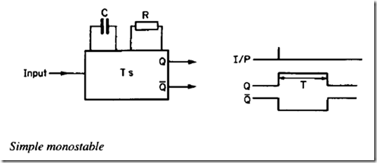
Control circuits often need time delays (e.g. open gas valve, run igniter for Ss, check for gas flame). Delays are often provided by circuits called monostables. In its simplest form, a !!!Onostable is as shown below. It has one input and the usual Q and Q outputs. In addition there are two components determining the period of the delay. Usually the period, T, is given approximately by 0.7 RC.
Every time the input goes from 0 to I, output Q goes from 0 to I for T seconds, then back to 0 again. Q does the opposite.
There are many variations in design of monostables. Common variants are shown in the timing charts. The delay on and delay off are obvious. The re-triggerable variant restarts the timing period for each 0 to I transition at the input.
The period of a monostable is of the order of RC seconds where R and C are the value of the timing components. Delays in excess of about 30 seconds consequently need large values of R or C. Practical limits for R are around I megohm or leakage becomes a problem. Large values of capacitance imply the use of electrolytics. These are bulky, have high leakage current and low accuracy.
The technique shown below allows long delays (up to years!) to be constructed with reasonable value components. An oscillator produces a free-running pulse train. This can be built around a normal timer IC and run at a relatively high frequency. The pulses are normally blocked by the AND gate.
To start the timer a pulse is applied to the input. This sets the S-R flip-flop and resets the counter. Pulses are now allowed to pass to the counter. When the counter reaches some predetermined value, the S R flip-flop is reset, blocking further pulses. The Q output of the flip flop is high for a time:
T = NP sees
where N is the counter preset and P the oscillator period. Time is accurate to one cycle of the oscillator.
Such a circuit is available in IC form, typical of which is the Ferranti ZN 1034 which includes the RC oscillator and a divide by 4096 counter.
Event-driven logic
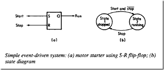
Most logic systems are not pure combinational logic, but incorporate storage and timer devices. Although such systems can be represented as shown earlier, output states are not determined solely by input conditions but also by what has happened previously. The simple motor start/stop circuit in (a), for example, has two inputs (start and stop buttons) and one output (motor run relay). The condition with no inputs present can, however, have the motor running or stopped according to which input was last present. Systems incorporating storage are often called event-driven or sequencing circuits.
Event-driven systems are designed around the concept of state diagrams. These show all the possible conditions that can exist for the system, identify the conditions that cause a change, and detail outputs in each state. The very simple state diagram for the motor starter is shown in (b), which shows that it has two states, with transitions between them being determined solely by the buttons. Note that with no button pressed the system can be in either state as explained before.
A more complex system for the control of a lift is shown in the facing page. This has eight inputs (two lift call buttons on the floors, two floor buttons in the lift, two limit switches saying the lift is at a floor, a door-closed limit switch, and a door-obstructed photocell) and four outputs (drive up/down, door open/close). There are eight possible states that the system can be in (states 3 and 7, for example, cover the condition where the lift is requested to move and someone is standing in the door).
Easiest way to go from the state diagram to a circuit is to assign a flip-flop to each state. Each is set by the entry conditions to the state, and reset by succeeding states. For example, (c) is the flip-flop for state I. Outputs are energised via OR gates. The door-open output, for example, is required in states I, 3, 5, 7 and is given by the circuit in (d).
State diagrams often incorporate timers. States 3 and 7 both start a five-second timer which initiates a retry at closing the door. Note that a given state may have routes to more than one succeeding state.
Event-driven systems are usually far more complex than that shown here (and there are many safety defects in the described lift control scheme!) but most can be converted to a circuit via a state diagram. The technique is also useful for the design of event-driven computer and programmable controller-based schemes.


Comments
Post a Comment