Positive and negative logic , Combinational logic and Boolean algebra.
Positive and negative logic
If the I voltage is more positive than the 0 voltage the logic is said to be positive logic. Consider for a moment the circuit in (a). If you followed the logic you would find that the output is I when inputs A and B are both I or inputs C and D are both I. It has thus behaved like the circuit in (b), and the right-hand NAND gate has somehow behaved like an OR gate.
The truth table for a NAND gate (given earlier), shows that the output is I if any input is 0. A positive logic NAND gate is thus also a negative logic NOR gate.
Similar interchangeability exists between all the logic gates, and these are now summarised.
Combinational logic
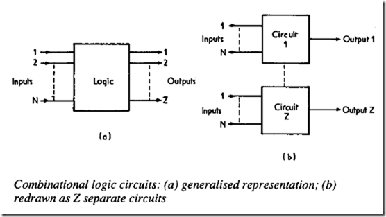
Circuits built purely around logic gates are called combinational logic circuits. These have no storage, counter or timer elements and can be represented as shown in (a). This has N inputs labelled I toN and Z outputs labelled I to Z. In systems with such multiple outputs it is often easier to consider the system as comprising Z separate, and different, circuits each of which can be represented as shown in (b).
The design of a combinational logic circuit consists first of defining in some way the relationship between inputs and output. This is then converted into a corresponding circuit built from logic gates.
One useful way of achieving this is via a truth table, in which all possible input states are tabulated along with the required outputs.
Suppose we wish to build a majority vote circuit where the output Z takes a majority vote of three inputs A, B, C. This would have the truth table:
It can be seen that Z is I for the four conditions marked with an asterisk, namely:
allowing us to build a circuit which is a series of AND gates whose outputs are OR'd together as shown.
Designs with truth tables always give an AND/OR solution that works (called a sum of products, or S ofP, circuit). What is not known, however, is whether the solution uses the minimum number of gates. To get to a minimal circuit other techniques must be used. Truth tables also tend to become rather unwieldy with more than four inputs (which have 16 possible input combinations).
Boolean algebra
In the nineteenth century a Cambridge mathematician and clergy man, George Boote, developed an algebraic notation system to express and manipulate logical expressions. His algebra can be used to design combinational logic circuits.
The AND function is represented by a dot(.), the OR function by a + symbol. The inverse (NOT) function is rep.!.esented by a bar above the signal, so NOT A is represented by A.
Using this Boolean notation the circuit shown can be represented
by:
Boolean algebra allows complex expressions to be written in a simple and concise form, but it also contains rules to allow expressions to be manipulated and a minimal form found.
To do this, a series of rules is used. The first eleven of these are really self-evident:
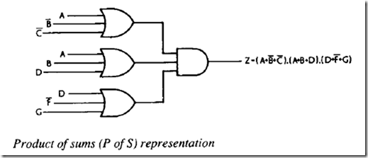
We have already encountered the S of P representation of a logic circuit. It is also possible to form a Product of Sums circuit which consists of a series of OR gates whose outputs are AND'd together, as shown.
The last two laws, known as De Morgan's theorem, give ways to go from S of P, toP of S forms and also how to form the inverse of any given expression:
As written out like this, De Morgan's theorem appears of little use. It can be more easily expressed in English:
'To form the complement of an expression there are two steps:
I replace each + by a . and each . by a +
2 complement each term in the original expression.'
For example, to complement:
which is the complement of the original expression (as can be verified by constructing the corresponding truth tables).
Boolean algebra can be used to minimise expressions, but it relies on intuition and there is no logical procedure. It is easy to make errors on double or triple inversions, and also in the swapping of the 'dot' and 'plus' symbols. As an example of the use of Boolean algebra to minimise an expression, consider:


Comments
Post a Comment