Inverting amplifier and Voltage follower.
Inverting amplifier
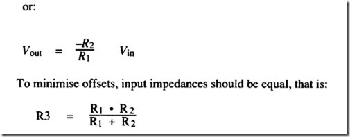
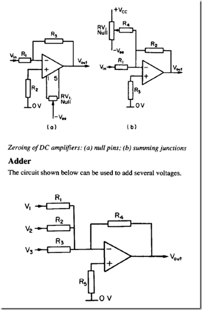
The circuit of an op-amp inverting amplifier is shown. As the gain of the amplifier is very high, it can be assumed that the junction of R 1 and R2 will be within a few millivolts of 0 V.
The amplifier can be zeroed for V10 and I10 by either of the two methods shown in (a) and (b). The first uses the null facility on the chip (pins I and 5 on the 741). The method shown in (b), however, uses an additional resistor R4, to add or subtract current to I1 •
By a similar analysis to that above:
and the value ofR5 is the parallel resistance ofR 1, R2, R3 and R4.
The adder circuit is used in analogue computers and as the basis
for audio mixers.
Voltage follower
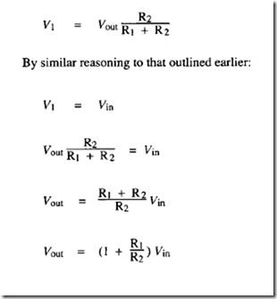
The circuit below applies I 00% feedback. As there can be only a millivolt or so between the inputs:
Input impedance is very high (typically several megohms), and output impedance very low (typically just a few ohms).
The circuit is a very useful buffer stage and can be considered an exceptionally efficient emitter follower.
Non-inverting amplifier
Various configurations of op-amp non-inverting amplifiers are shown over. Ana lysing the circuit in (a), we see that the voltage at the inverting input is given by:
AC audio amplifiers are commonly based on the circuit of (a). In (b), capacitors C 1 and C2 provide AC isolation, while resistors R 1 and R2 define the DC level of the non-inverting input and the output. AC gain is determined by resistors R3 and R4.
The input impedance of (b) is given by R1 in parallel with R2. The bootstrapped circuit of (c) gives a very high input impedance. DC levels are set by resistors R 1 and R2 as before.
Differential amplifier
It is frequently required to measure the difference between two voltages. An example is the strain gauge bridge shown. X 1 and X2 are two strain gauges to be measured, arranged such that X 1 increases in resistance for increasing stress while decreases. Y 1 and Y2 are identical strain gauges not under stress, included to provide temperature compensation.
Voltage V8 is the bridge voltage, which in practice is very small. When it arrives at the amplifier, the voltage at each input is:
where Vern is common mode noise induced on the lines from external sources of interference.
If the leads are run from the bridge as a screened twisted pair, the common mode voltage is the same at both inputs, allowing a differential amplifier to be used.
A differential amplifier circuit is shown. It is very important, for correct operation, that resistors R 1 = R3 and R2 = R4. If these conditions are met:
For maximum CMRR, precision resistors should be used.
Differential amplifiers are widely used where low voltage signals (e.g. in thermocouples, strain gauges, medical electronics) have to be amplified in the presence of common mode interference.


Comments
Post a Comment