Cells and batteries, AC amplifiers and Basic principles.
Cells and batteries
AC amplifiers
It is possible that the commonest types of electronic circuit are those covered by the term amplifier. The description AC amplifier covers a wide range of circuits, from the domestic hi-fi system to radio circuits operating at frequencies of over 1000 MHz. This section first describes the basic principles of AC amplification, then discusses specific amplifier types.
Basic principles
The basic requirements of an amplifier are simple. It is a circuit with two input terminals and two output terminals, as shown.
An alternating voltage, Vm, is applied to the input terminals and an amplified copy, Vout, appears at the output terminals. To describe the amplifier operation we need to define the following terms.
Frequency and period
The frequency of a signal is defined as the number of cycles of the signal occurring in Is. The sine wave shown repeats every 1 ms. It therefore has a period of 1 ms and a frequency of 1 kHz.
Harmonie content
Most of the waveforms encountered in practice are vastly different from a pure sine wave, and in many cases (such as speech) it is almost impossible to define a fundamental frequency. It can be shown, however, that any repetitive waveform can be constructed by the addition of a series of sine and cosine waves at fundamental frequency, 2 x fundamental, 3 x fundamental and so on. These are known as the harmonics of the waveform. It is the different harmonic content that makes middle C on a violin sound different from middle C on, say, a piano. In general, the higher the frequency of the harmonic, the smaller its amplitude. There comes a point, therefore, when the higher frequency components become so small as to be negligible. The technique of splitting a complex waveform into its component frequencies is called Fourier analysis. Examples are shown.
The technique has important implications for AC amplifier design. If it is desired to amplify a complex signal, a Fourier analysis will show the range of frequencies contained in the signal. If the amplifier performance is consistent over this range, the output signal will be an amplified true replica of the input signal. In an audio amplifier, for example, we need to cover frequencies from 30 Hz to over 15 kHz if we are to provide a true rendering of a musical performance.
Gain
The gain is defined for one specific frequency because desired, and undesired, effects will cause it to be different at other frequencies. In many amplifier circuits, gains of several thousand are common, and it is more convenient to express gains in logarithmic terms. Amplifier gains are often expressed in decibels, defined as a power ratio:
Although this expression is only strictly true if source and load impedance are equal, amplifier gains are often (incorrectly) expressed in decibels when source and load impedances are different.
Bandwidth
It was mentioned earlier that an amplifier’s gain is specified at one particular frequency, and that the gain is different at other frequenP cies.At low frequencies, coupling capacitors between amplifier stages increase in impedance, causing loss of gain. At high frequencies the gain is reduced by stray capacitance and limitations of the transistors themselves.
It therefore follows that a graph of gain versus frequency would appear similar to that shown. It is usual to define the range of frequencies over which the amplifier can be used as the amplifier bandwidth. Normally this is taken between the two points at which the gain has fallen by 3 dB (i.e. where power gain has fallen by half).
In many amplifier circuits (notably radio circuits) the bandwidth is deliberately designed to amplify, or reject, one particular range of frequencies.
Basic transistor amplifiers
A single transistor amplifier stage can be arranged in any of the three configurations shown. These are known as common emitter, common collector and common base.
Common emitter amplifier
The most popular form of amplifier circuit is the common emitter. In its simplest form it is arranged as in (a). To keep a transistor conducting with current flow from collector to emitter, a much smaller current has to flow from'base to emitter and under these conditions a voltage exists between emitter and base of approxiP mately 0.6 V.
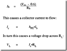
The ratio of collector current to base current is called the common emitter current gain, and has the symbol hFE (or sometimes the Greek letter K ). Values of hpg vary greatly, even within the same type of transistor. For example, the common audio transistor BC108 can have an in the range 100 to 800. In (a), base current is provided by Rb and is given by:
Ideally RL and Rb are chosen such that VL = 0.5 Vcc, allowing an equal positive or negative swing of voltage at the collector. If a small AC signal is now applied to the base, the base current will change in sympathy, causing a larger change in collector current. This, in turn, produces a large voltage change across RL. Note that a positive increase in voltage at the base causes more base current to flow, causing more collector current to flow and the collector voltage to fall. The amplified output is the inverse of the input signal.
This simple amplifier circuit has many shortcomings. The values of Rb and RL have to be adapted very precisely to the characteristics of the particular transistor. As mentioned earlier varies widely from transistor to transistor, even of the same nominal type. Of more importance, however, is the sad fact that transistor characteristics are very temperature-dependent. A simple circuit such as in (a) would not, in fact, work reliably over a temperature range of more than a few degrees Centigrade. There are several transistor parameters that are temperature dependent, but the most important are the current gain and the collector to emitter leakage current. The leakage current (denoted /ceo) is the current flowing from collector to emitter with the base disconnected. This current is highly temperature-dependent and doubles for each 8°C rise. An improvement can be made with the circuit shown in (b). The base resistor Rb is now returned to the collector. Suppose we have chosen Rb and RL such that the collector is sitting correctly at 0.5 Vcc, and changes in temperature cause the leakage current to rise. The change in leakage current causes more collector current to flow, causing the collector volts to fall. The fall in collector volts reduces the base current flowing through Rb, reducing the collector current and compensating, to some extent, for the change in leakage current. The circuit shown in (c) gives almost perfect compensation for changes in transistor characteristics. Resistors Rbl and Rb2 are a voltage divider defining the base voltage. The emitter voltage is thus defined, as the base emitter voltage is effectively constant at 0.6 V.
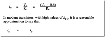
Because the emitter voltage is fixed, the emitter current is given by:
Hence the voltage drop across RL is defined.
In this particular circuit arrangement, variations in hpg only affect the base current being drawn from the voltage divider Rbl, Rb2. The variation in base current causes a negligible change in operating conditions if the standing bleed current through Rbl, Rb2 is significantly larger than the base current. Resistors Rbl and Rb2 must not be made too small, however, or the input impedance of the stage will be unacceptably low.
Calculation of the gain of a single-stage amplifier can be made very mathematical, with complex models. For most purposes, however, simple approximations give adequate accuracy. To define the gain of our single-stage amplifier we need two parameters. The first is Afc. This is similar to the DC gain h^ above, with the exception that it is the small signal AC gain (or AC ß ), that is:
where ª denotes small change. The parameter hfe is a ratio (and hence is dimensionless) and has a typical range of 50 to 800. The second parameter is Aie. This relates the variation of base current to small signal changes in base emitter voltage. It is defined as:
The parameter Aie has the dimensions of resistance, and has a typical value of several hundred ohms. In the following equations, load resistor RL is not simply the collector load resistor; it is the effective parallel resistance of the collector resistor Rc and the input resistance Rjn of the stage following, that is:
For the voltage amplifier of (c), we can use the following equations to give an adequate approximation of performance:
In equation (1), the effect of Re is to raise the input impedance. In equation (3), the effect of Re is to lower the gain. In most circuits the value of h-Jhit is much less than Re, so equation (3) can be simplified to:
In most amplifier circuits, however, the degradation of gain due to Re is not acceptable. If an emitter decoupling capacitor Ce is added as shown in (c), the DC conditions necessary to give stable operation are unchanged, but the effective emitter impedance to AC signals becomes almost zero. Substituting Re = 0 into equation (3), we get:
The ratio hfe/hie is sometimes given the symbol gm. Equation (4) assumes that the decoupling capacitor Ce has negligible impedance compared with hlfJhfe. The impedance of a capacitor increases with decreasing frequency; hence the requisite value of Ce must be calculated for the lowest frequency to be amplified. Transistor characteristics vary greatly from device to device, so the above formula can only be used as a guide to expected results. In practical amplifier designs it is usual to design an amplifier with very high gain, and then use feedback (described later) to define the gain. In this way, consistent amplifier performP ance can be obtained over the full tolerance of characteristics.


Comments
Post a Comment