Operational Amplifiers part3
INTEGRATORS AND DIFFERENTIATORS
The op-amp circuit applications discussed so far, utilized resistors in the op-amp feedback path and in connecting the signal source to the circuit, that is, in the feed-in path. As a result circuit operation has been (ideally) independent of frequency. The only exception has been the use of coupling capacitors in order to minimize the effect of the dc imperfections of op amps. By allowing the use of capacitors together with resistors in the feedback and feed-in paths of op-amp circuits, a very wide range of useful and exciting applications of the op amp can be obtained. We begin our study of op-amp-RC circuits in this section by considering two basic applications, namely signal integrators and differentiators.
The Inverting Configuration with General Impedances
Consider the inverting closed-loop configuration with impedances and replacing resistors R1 and R2, respectively. The resulting circuit is shown in Fig. 5.44 and, for an ideal op amp, has the closed-loop gain or, more appropriately, the closed-loop transfer function
5.60
Replacing s by provides the transfer function for physical frequencies , that is, the transmission magnitude and phase for a sinusoidal input signal of frequency
Figure 5.44 The inverting configuration with general impedances in the feedback and the feed-in paths.
The Inverting Integrator
By placing a capacitor in the feedback path (i.e.in place of in Fig.5.44) and a resistor at the input (in place of , we obtain the circuit of Fig. 2.45(a). We shall now show that this circuit realizes the mathematical operation of integration. Let the input be a time- varying function . The virtual ground at the inverting op-amp input causes to appear in effect across R, and thus the current will be . This current flows through the capacitor C, causing charge to accumulate on C. If we assume that the circuit begins operation at time t = 0, then at an arbitrary time t the current will have deposited on C a charge equal to Thus the capacitor voltage will change by lf the initial voltage on C (at t = 0) is denoted , then
Now the output voltage thus,
(a)
Figure 5.45. (a) The Miller or inverting integrator. (b) Frequency Response of the Integrator
Thus the circuit provides an output voltage that is proportional to the time-integral of the input, with being the initial condition of integration and CR the integrator time- constant. The negative sign attached to the output voltage, indicates that the circuit is an inverting integrator. It is also known as a Miller integrator.
The operation of the integrator circuit can be described alternatively in the frequency domain by substituting and in Eq. (5.60) to obtain the transfer function
The Bode plot for the integrator magnitude response can be obtained by noting from Eq.(5.63) that as doubles (increases by an octave), the magnitude is halved (decreased by 6 dB).Thus the Bode plot is a straight line of slope -6 dB/octave (or, equivalently, -20 dB/decade). This line [shown in Fig. 5.45(b)] intercepts the 0- dB line at the frequency that makes = 1, which from Eq. (5.63) is
(5.64)
The frequency is known as the integrator frequency and is simply the inverse of the integrator time constant.
Comparison of the frequency response of the integrator to that of an STC low-pass network indicates that the integrator behaves as a low-pass filter with a corner frequency of zero. Observe also that at = 0, the magnitude of the integrator transfer function is infinite. This indicates that at dc the op amp is operating with an open loop. Reference to Fig. 5.45(a) shows that the feedback element is a capacitor, and thus at dc, where the capacitor behaves as an open circuit, there is no negative feedback! This is a very significant observation and one that indicates a source of problems with the integrator circuit: Any tiny dc component in the input signal will theoretically produce an infinite output, resulting in the output of the amplifier saturating at a voltage close to the op-amp positive or negative power supply (L+ or L-), depending on the polarity of the input dc signal.
To see the effect of the input dc offset voltage consider the integrator circuit in Fig. 5.46, where for simplicity we have short-circuited the input signal source. Analysis of the circuit is straightforward and is shown in Fig. 5.46. Assuming for simplicity that at time t = 0 the voltage across the capacitor is zero, the output voltage as a function of time is given by
Figure 5.46 Determining the effect of the op-amp input offset voltage VOS on the Miller integrator circuit. Note that since the output rises with time, the op amp eventually saturates.
Thus increases linearly with time until the op amp saturates which is unacceptable. Similarly, the dc input offset current produces a similar problem. Figure 5.47 illustrates the situation. Observe that we have added a resistance R in the op-amp positive- input lead in order to keep the input bias current from flowing through C.
Figure 5.47 Effect of the op-amp input bias and offset currents on the performance of the Miller integrator circuit.
Nevertheless, the offset current will flow through C and cause to ramp linearly with time until the op amp saturates.
Figure 5.48 Eliminating the DC problem in Integrator
The dc problem of the integrator circuit can be alleviated by connecting a resistor across the integrator capacitor C, as shown in Fig, 5.48. Such a resistor provides a dc path through which the dc currents and can flow, with the result that will now have a dc component instead of rising linearly. To keep the dc offset at the output small, one would select a low value for . However, the lower the value of , the less ideal the integrator circuit becomes. This is because causes the frequency the integrator pole lo move from its ideal location at =0 to one determined by the comer frequency of the STC network (,C). Specifically, the integrator transfer function becomes as opposed to the ideal function of . The lower the value of , the higher the corner frequency (), and the more non-ideal the integrator becomes. Thus selecting a value for presents the designer with a trade-off between dc performance and signal performance. Observe that closes the negative-feedback loop at dc and provides the integrator circuit with a finite dc gain of .
The Op-Amp Differentiator
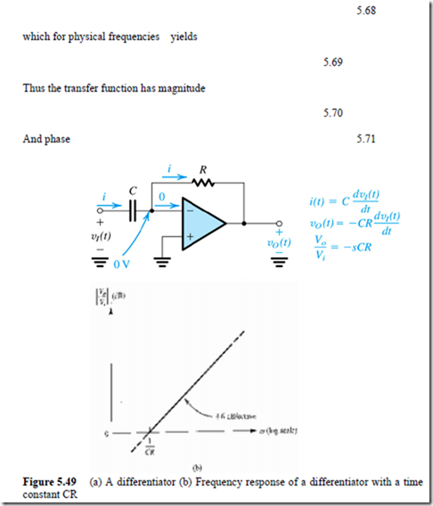
Interchanging the location of the capacitor and the resistor of the integrator circuit results in the circuit in Fig. 5.49(a), which performs the mathematical function of differentiation. To see how this comes about, let the input be the time-varying function and note that the virtual ground at the inverting input terminal of the op amp causes to appear in effect across the capacitor C. Thus the current through C will be and this current flows through the feedback resistor R providing at the op-amp output a voltage ,
The frequency-domain transfer function of the differentiator circuit can be found by substituting in Eq. (5.60), obtain
The Bode plot of the magnitude response can be found from Eq. (5.70) by noting that for an octave increase in , the magnitude doubles (increases by 6 dB). Thus the plot is simply a straight line of slope +6 dB/octave (or, equivalently, +20 dB/decade) intersecting the 0-dB line (where = 1) at l/CR, where CR is the differentiator time-constant [see Fig. 5.49(b)|.
The frequency response of the differentiator can be thought of as that of an STC highpass filter with a corner frequency at infinity. Finally, we should note that the very nature of a differentiator circuit causes it to be a "noise magnifier." This is due to the spike introduced at the output every time there is a sharp change in ; such a change could be interference coupled electromagnetically ("picked-up") from adjacent signal sources. For this reason and because they suffer from stability problems, differentiator circuits are generally avoided in practice. When the circuit of Fig. 5.49(a) is used, it is usually necessary to connect a small-valued resistor in series with the capacitor. This modification turns the circuit into a non-ideal differentiator.
NONLINEAR FUNCTION OPERATIONS
There are many useful applications where opamps find their use as nonlinear devices basically operating in the saturation regions, [ ±.Some of them are logarithmic and anti- logarithmic amplifiers, analog multipliers and sample and hold circuits.
Logarithmic Amplifiers
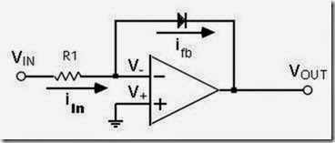
They are nonlinear circuits where the output voltage is the logarithm of the input signal. It is basically an inverting amplifier where the feedback resistor is replaced with a p-n junction diode.
Figure 5.50 Circuit for a Logarithmic amplifier
The V-I relation of a p-n diode is
Where is the forward current of the diode, is the reverse saturation current, is the voltage across the diode, is the thermal voltage, and ή is 1 for Si diode and 2 for Ge diode. Restricting the operating range of the diode such that then, neglecting ,
If we take the logarithm on both sides,
Hence, it is seen that the voltage across a diode is proportional to the logarithm of the current flowing through it.
Now, consider the logarithmic amplifier shown in Fig. 5.55.From the virtual ground concept inverting terminal is also at virtual ground. Therefore, the output voltage of the circuit is
5.76
Where is the current flowing through the diode and same as current through , as current entering into opamp input terminal is negligible. Hence is given by
5.77
Substituting Eq.(5.77) in Eq. (5.76), we get
5.78
Hence, the output of a logarithmic amplifier is proportional to the input voltage. But, it contains two temperature dependent terms, the scaling factor ‘and the offset term Hence the above logarithmic amplifier is very sensitive to temperature. To minimize this the circuit is modified as shown below:
Figure 5.51 Circuit for a Temperature Compensated Logarithmic amplifier
Here two matched diodes are used to cancel the temperature dependent offset term . Then, a thermistor (temperature dependent resistor) is used to cancel the temperature dependent scaling factor .The output voltage of op amp A1 is negative of voltage across diode D1 and is given by
5.79
Similarly, the voltage across diode D2 is given by,
5.80
As both diodes are matched, their reverse saturation currents are the same. The voltage at non-inverting terminal of opamp A2 is,
5.81
Thus, temperature dependent offset term is eliminated from the output of a1.The op amp A2 is a non inverting amplifier and its output is given by,
5.82
5.83
Hence the above circuit provides a temperature independent logarithmic output.
Note: The dynamic range of the op amp is limited by the non-ideal characteristics of op amps.
Antilogarithmic Amplifiers
Antilogarithmic amplifiers produce an output that is an antilogarithm of its input. It uses two diodes and two op amps as shown in Figure 5.58. Matched diodes D1 and D2 are used to minimize the effect of temperature dependent reverse saturation current on the output. The current source I is connected to the inverting input of A1 and the input signal is connected to the non inverting terminal through a voltage divider network, comprising of and .The output of op amp A1 due to the current source is given by,
5.84
The output due to the input source is given by,
5.85
The output voltage due to both sources is given by,
5.86
Similarly, the voltage across diode D2, is given by
5.87
Figure 5.52 Circuit for an Antilogarithmic amplifier
Where I is the forward current through D2 and Is is the reverse saturation current, which is same as that through D1.Equating 5.86 and 5.87 gives,
5.88
5.89
Taking the antilogarithm of both sides,
5.90
As shown in the figure current I is the output current through .Hence, the output voltage is given by,
5.91
Note: The effect of the temperature dependent term can be eliminated if the resistive network is made dependent on temperature.
The dynamic performance of antilog amplifiers is also limited by the input offset voltage, input bias current and input noise of both op amps.
Analog Multipliers
The fundamental logarithmic relationship that the addition of two logarithmic terms is equal to the logarithm of the multiplication product of the two terms forms the basis for analog multipliers. If are the two input signals to be multiplied, using logarithms, we get,
5.92
5.93
The above equations can be used to implement analog multiplier as shown below:
Figure 5.53 Basic block diagram of an analog multiplier
Sample and Hold (S & H) Circuit
They are widely used in applications such as analog to digital (A –D) converters. The A- D converter takes very little time for the conversion, during which the analog input signal should remain constant. The S & H circuit serves this purpose. It basically samples the input signal and holds on to the last sampled signal value. The schematic diagram of a basic S & H circuit is as shown below:
Figure 5.54 Basic S & H circuit
The switch S, generally made using a device such as MOSFET, is connected in series with the input, and the Capacitor C is connected across the output as shown in Figure
5.54. Whenever the switch is closed, the input signal is connected to the output and hence the voltage across the capacitor, the output voltage is same as the input. This mode of operation is called the sample mode. When the switch is open, the input signal is disconnected from the output and the previous sampled value is held till the switch is closed again.
The schematic diagram of a S & H circuit using two op amps is as shown below:
Figure 5.55 S & H circuit using Op amps
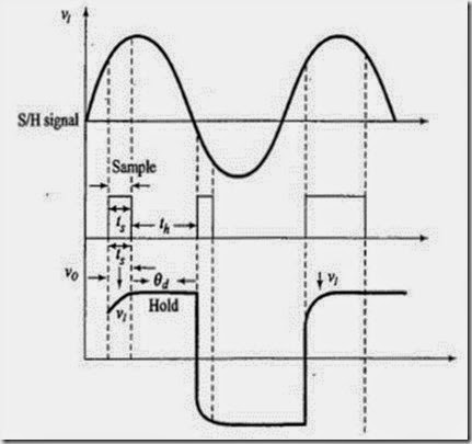
Working: The MOSFET works as a switch and is controlled by the voltage , and the capacitor stores the charge. Both op amps are configured as Voltage followers. The input voltage, which is same as output of A1, is applied at the drain of the MOSFET M1.The control voltage is applied to the gate. When control voltage is positive, M1 is on and the capacitor C gets charged instantaneously to .This appears across the second op amp whose output follows the input. When voltage is zero, M1 is off. Capacitor is disconnected from the input and cannot discharge as it faces the high input impedance of the voltage follower A2.Thus the capacitor holds the voltage across it as shown. The time period , known as the sample period is the time during which the voltage across the capacitor is equal to the input voltage. The time known as the hold period, is the time during which the voltage across the capacitor is held constant.
Figure 5.56 Waveforms for S & H circuit using Op amps


Comments
Post a Comment