Digital cmos logic circuits:digital circuit design: an overview,design and performance analysis of the cmos inverter and cmos logic-gate circuits.
Digital CMOS Logic Circuits
In summary, this chapter provides a reasonably comprehensive and in-depth of CMOS digital integrated-circuit design, perhaps the most significant area (at least in terms of production volume and societal impact) of electronic circuits.
1. DIGITAL CIRCUIT DESIGN: AN OVERVIEW
We discuss the various technologies and logic-circuit families currently in use, consider the parameters employed to characterize the operation and performance of logic circuits, and finally mention the various styles for digital-system design.
1.1. Digital IC Technologies and Logic-Circuit Families
The chart in Figure 1 shows the major IC technologies and logic-circuit families that are currently in use. Members of each family are made with the same technology, have a similar circuit structure, and exhibit the same basic features. Each logic- circuit family offers a unique set of advantages and disadvantages. In the conventional style of designing systems, one selects an appropriate logic family (e.g., TTL, CMOS, or ECL) and attempts to implement as much of the system as possible using circuit modules (packages) that belong to this family. In this way, interconnection of the various packages is relatively straightforward.
The selection of a logic family is based on such considerations as logic flexibility, speed of operation, availability of complex functions, noise immunity, operating-temperature range, power dissipation, and cost.
Figure 1 Digital IC technologies and logic-circuit families.
CMOS technology is, by a large margin, the most dominant of all the IC technologies available for digital-circuit design. As mentioned earlier, CMOS has replaced NMOS, which was employed in the early days of VLSI (in the 1970s). The most important of which is the much lower power dissipation of CMOS circuits. CMOS has also replaced bipolar as the technology-of-choice in digital-system design, and has made possible levels of integration (or circuit-packing densities), and a range of applications, neither of which would have been possible with bi-polar technology.
1. CMOS logic circuits dissipate much less power than bipolar logic circuits and thus one can pack more CMOS circuits on a chip than is possible with bipolar circuits.
2. The high input impedance of the MOS transistor allows the designer to use charge storage as a means for the temporary storage of information in both logic and memory circuits. This technique cannot be used in bipolar circuits.
3. The feature size (i.e., minimum channel length) of the MOS transistor has decreased dramatically over the years, with some recently reported designs utilizing channel lengths as short as 0.06 µm. This permits very tight circuit packing and, correspondingly, very high levels of integration.
Bipolar Two logic-circuit families based on the bipolar junction transistor are in some use at present: TTL and ECL, Transistor-transistor logic (TTL or T2L) was for many years the most widely used logic-circuit family. Its decline was precipitated by the advent of the VLSI era. TTL manufacturers, however, fought back with the introduction of low-power and high-speed versions. In these newer versions, the higher speeds of operation are made possible by preventing the BIT from saturating and thus avoiding the slow turnoff process of a saturated transistor. These nonsaturating versions of TTL utilize the Schottky diode and are called Schottky TTL. Despite all these efforts, TTL is no longer a significant logic-circuit family
The other bipolar logic-circuit family in present use is emitter-coupled logic (ECL). It is based on the current-switch implementation of the inverter, The basic element of ECL is the differential BIT pair, and, correspondingly, also called current- mode logic (CML), in which saturation is avoided, very high speeds of operation are possible. Indeed, of all the commercially available logic-circuit families, ECL is the fastest. ECL is also used in VLSI circuit design when very high operating speeds are required and the designer is willing to accept higher power dissipation and increased silicon area.
BiCMOS BiCMOS combines the high operating speeds possible with BJTs (because of their inherently higher transconductance) with the low power dissipation and other excellent characteristics of CMOS. Like CMOS, BiCMOS allows for the implementation of both analog and digital circuits on the same chip. At present, BiCMOS is used to great advantage in special applications, including memory chips, where it requires a high-speed and lower power dissipation.
Gallium Arsenide (GaAs) The high carrier mobility in GaAs results in very high speeds of operation. This has been demonstrated in a number of digital IC chips utilizing GaAs technology. It should be pointed out, however, that GaAs remains an "emerging technology," one that appears to have great potential but has not yet achieved such potential commercially.
1.2. Logic-Circuit Characterization
The following parameters are usually used to characterize the operation and performance of a logic-circuit family.
Noise Margins The static operation of a logic-circuit family is characterized by the voltage transfer characteristic (VTC) of its basic inverter. Figure 2 shows such a VTC and defines its four parameters; VOH. VOL, VIH and VIL Note that VIH and VIL are defined as the points at which the slope of the VTC is -1, Also indicated is the definition of the threshold voltage VM or Vth as we shall frequently call it, as the point at which VO = Vi .
The robustness of a logic-circuit family is determined by its ability to reject noise, and thus by the noise margins NHH and NML,
NMH = VOH - VIH (1)
NML = VIL - VOL (2)
Figure 2 Typical voltage transfer characteristic (VTC) of a logic inverter, illustrating the definition of the critical points.
An ideal inverter is one for which NMH= NML=VDD/2,where VDD is the power- supply voltage. Further, for an ideal inverter, the threshold voltage VM= VDD/2.
Propagation Delay The dynamic performance of a logic-circuit family is characterized by the propagation delay of its basic inverter. Figure 3 illustrates the definition of the low-to-high propagation delay (tPLH) and the high-to-low propagation delay (tPHL) The inverter propagation delay (tP) is defined as the average of these two quantities:
tP= ½ (tPLH+ tPHL) (3)
Figure 3 Definitions of propagation delays and switching times of the logic inverter.
Power Dissipation The need to minimize the gate power dissipation is motivated by the desire to pack an ever increasing number of gates on a chip, which in turn is motivated by space and economic considerations. Modern digital systems utilize large numbers of gates and memory cells, and thus to keep the total power requirement within reasonable bounds, the power dissipation per gate and per memory cell should be kept as low as possible.
There are two types of power dissipation in a logic gate: static and dynamic. Static power refers to the power that the gate dissipates in the absence of switching action. It results from the presence of a path in the gate circuit between the power supply and ground in one or both of its two states.Dynamic power, on the other hand, occurs only when the gate is switched: An inverter operated from a power supply VDD and driving a load capacitance C, dissipates dynamic power PD,
PD =f CVDD2 (A)
Where f is the frequency at which the inverter is being switched.
Delay-Power Product One is usually interested in high-.speed performance (low tP) combined with low power dissipation. Unfortunately, these two requirements are often in conflict; when designing a gate, if one attempts to reduce power dissipation by decreasing the supply voltage, or the supply current, or both, the current-driving capability of the gate decreases. This in turn results in longer times to charge and discharge the load and parasitic capacitances, and thus the propagation delay increases.
DP =PD tP (B)
where PD is the power dissipation of the gate. Note that DP has the units of joules. The lower the DP figure for a logic family, the more effective it is.
Silicon Area Objective in the design of digital VLSI circuits is the minimization of silicon area per logic gate. Smaller area requirement enables the fabrication of a larger number of gates per chip, which has economic and space advantages from a system design standpoint. Area reduction occurs in three different ways: through advances in processing technology, through advances in circuit-design techniques, and through careful chip layout. In this book, our interest lies in circuit design. As a general rule, the simpler the circuit, the smaller the area required.
The circuit designer has to decide on device sizes. Choosing smaller devices has the obvious advantage of requiring smaller silicon area and at the same time reducing parasitic capacitances and thus increasing speed. Smaller devices, however,have lower current-driving capability, which tends to increase delay. Thus, as in all engineering design problems, there is a trade-off between speed and area.
Fan-In and Fan-Out The fan-in of a gate is the number of its inputs. Thus, a four- input NOR gate has a fan-in of 4. Fan-out is the maximum number of similar gates that a gate can drive while remaining within guaranteed specifications.
1.3. Styles for Digital System Design
The conventional approach to designing digital systems consists of assembling the system using standard IC packages of Various levels of complexity (and hence integration). The advent of VLSI, in addition to providing the system designer with more powerful off-the-shelf components such as microprocessors and memory chips, has made possible alternative design styles. One such alternative is to opt for implementing part or all of the system using one or more custom VLSI chips.
IC Technology is the manner in which a digital (gate-level) implementation is mapped on to an IC. IC’s consist of numerous layers (perhaps 10 or more)
The three main IC technologies are:
1) Full-custom/VLSI:
• All layers are optimized for an embedded system’s particular digital implementation
* Placing transistors Y Sizing transistors Y Routing wires
• Benefits
* Excellent performance, small size, low power
• Drawbacks
* Long time-to-market
2) Semi-custom ASIC(gate array and standard cell)
• Lower layers are fully or partially built
* Designers are left with routing of wires and may be placing some blocks
• Benefits
*Good performance, good size.
• Drawbacks
* Still require weeks to months to develop
3) PLD(Programmable Logic Device)
• All layers are already exist
* Designers can purchase an IC
* Connection on the IC are either created or destroyed to implement desired functionality. Field-Programmable Gate Array(FPGA) very popular
• Benefits
* Almost instant IC availability
• Drawbacks
* Bigger, expensive, power hungry, slower
1.4 Design Abstraction and computer Aids
2. DESIGN AND PERFORMANCE ANALYSIS OF THE CMOS INVERTER
2.1 Circuit Structure
The inverter circuit, shown in Fig. 4(a), consists of a pair of complementary MOSFETs switched by the input voltage VI. Although not shown, the source of each device is connected to its body, thus eliminating the body effect. Usually, the threshold voltages Vtn and Vtp are equal in magnitude; that is, Vtn=|Vtp| = Vt is in the range of 0.2 V to 1 V. The inverter circuit can be represented by a pair of switches operated in a complementary fashion, as shown in Fig. 4(b). As indicated, each switch is modeled by a finite on resistance, which is the source-drain resistance of the respective Transistor, evaluated near | VDS| = 0.
2.2 Static Operation
Case 1: With VI = 0, VO=VOH=VDD, and the output node is connected to VDD through the resistance rDSP of the pull-up transistor QP.
Case 2: with VI = VDD , VO=VOL=0, and the output node is connected to ground through the resistance rDSN of the pull-down transistor QN.
Thus, in the steady state, no direct-current path exists between VDD and ground, and the static-current and the static-power dissipation are both zero (leakage effects are usually negligibly small particularly for large-feature-size devices).
The voltage transfer characteristic of the inverter is shown in Fig. 5, from which it is confirmed that the output voltage levels are 0 and VDD, and thus the output voltage swing is the maximum possible. The fact that VOH and VOL are independent of device dimensions makes CMOS very different from other forms of MOS logic.
The CMOS inverter can be made to switch at the midpoint of the logic swing, 0 to VDD, that is, at VDD/2, by appropriately sizing the transistors. Specifically, it can be shown that the switching threshold Vth (or VM) is given by
Thus a symmetrical transfer characteristic is obtained when the devices are designed to have equal trans conductance parameters, a condition we refer to as matching. Since µn is two to four times larger than µP, matching is achieved by making (W/ L)p two to four times (i.e., µn / µP times) (W/L)n,
The two devices have the same channel length, L, which is set at the minimum allowable for the given process technology. The minimum width of the NMOS transistor is usually one and a half to two times L, and the width of the PMOS transistor two to three times that. Since the inverter area can be represented by WnLn+ WpLp =(Wn + Wp)L, the area of the minimum-size inverter is(n +p)L2, and we can use the factor (n +P) as a proxy for area.
Besides placing the gate threshold at the center of the logic swing, matching the transconductance parameters of QN and Qp provides the inverter with equal current-driving capability in both directions (pull-up and pull-down).
Furthermore, and obviously related, it makes rDSN = rDSP. Thus an inverter with matched transistors will have equal propagation delays, tPLH and tPHL.
When the inverter threshold is at VDD/2, the noise margins NMH and NML are equalized, and their values are maximized, such that
A final comment on the inverter VTC, we note that the slope in the transition region,though large, is finite and is given by -(gmN + gmP)(roN||roP).
2.3 Dynamic Operation
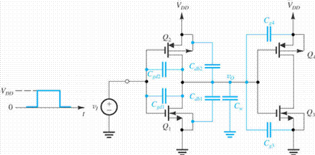
The propagation delay of the inverter is usually determined under the condition that it is driving an identical inverter. This situation is depicted in Fig. 6. The propagation delay of the inverter comprising Q1 and Q2, which is driven by a low-impedance source VI, and is loaded by the inverter comprising Q3 and Q4.
Indicated in the figure are the various transistor internal capacitances that are connected to the output node of the (Q1, Q2) inverter.
Replace all the capacitances attached to the inverter output node with a single capacitance C connected between the output node and ground. If we are able to do that, we can utilize the results of the transient analysis performed in Section 4.10. during tPLH or tPHL, the output of the first inverter changes from 0 to VDD/2 or from VDD to VDD/2 respectively. It follows that the second inverter remains in the same state during each of our analysis intervals.
Figure 6 Circuit for analyzing the propagation delay of the inverter formed by Q1 and Q2, which is driving an identical inverter formed byQ3 and Q4.
1. The gate-drain overlap capacitance of Q1, Cgd1, can be replaced by an equivalent capacitance between the output node and ground of 2Cgd1.The factor 2 arises because of the Miller effect (Section 6,4.4). Specifically, note that as VI goes high and VO goes low by the same amount, the change in voltage across Cgd1 is twice that amount.
Thus the output node sees in effect twice the value of Cgd1. The same applies for the gate drain overlap capacitance of Q2, Cgd2,which can be replaced by a capacitance 2 Cgd2 between the output node and ground.
2. Each of the drain-body capacitances Cdb1 and Cdb2 has a terminal at a constant voltage. Thus for the purpose of our analysis here, Cdb1 and Cdb2 can be replaced with equal capacitances between the output node and ground.
3. Since the second inverter does not switch states, we will assume that the input capacitances of Q3 and Q4remain approximately constant and equal to the total gate capacitance (WLCOX+ Cgsov + Cgdov). The input capacitance of the load inverter will be
An expression for the low-to –high inverter delay, tPLH, can be written by analogy to the tPHL expression in equation (16),
Examination of the formulas in Eqs. (16) and (17) enables us to make a number of useful observations:
1. As expected, the two components of tp can be equalized by selecting the (W/L) ratios to equalize kn and kp that is, by matching QN and QP.
2. Since tP is proportional to C, the designer should strive to reduce C. This is achieved by using the minimum possible channel length and by minimizing wiring and other parasitic capacitances.
3. Using a process technology with larger transconductance parameter k' can result in shorter propagation delays.
4. Using larger (W/L) ratios can result in a reduction in tp. However, should b exercised here also, since increasing the size of the devices increases the value of C, and thus the expected reduction in tp might not materialize.
5. A larger supply voltage VDD results in a lower tp. However, VDD is determined by the process technology and thus is often not under the control of the designer. These observations clearly illustrate the conflicting requirements and the trade-offs available in the design of a CMOS digital integrated circuit (and indeed in any engineering design problem),
2.4 Dynamic Power Dissipation
The dynamic power dissipated in the CMOS inverter is given by
PD = fCV2DD (18)
Where f is the frequency at which the gate is switched. It follows that minimizing C is an effective means for reducing dynamic-power dissipation. An even more effective strategy is the use of a lower power-supply voltage.
3. CMOS LOGIC-GATE CIRCUITS
3.1 Basic Structure
A CMOS logic circuit is in effect an extension, or a generalization, of the CMOS inverter:
The CMOS logic gate consists of two networks: the pull-down network (PDN) constructed of NMOS transistors, and the pull-up network (PUN) constructed of PMOS transistors (see Fig. 8). The two networks are operated by the input variables, in a complementary fashion. Thus, for the three-input gate represented in Fig. 8, the PDN will conduct for all input combinations that require a low-output (Y= 0) and will then pull the output node down to ground, causing a zero voltage to appear at the output, VY= 0. Simultaneously, the PUN will be off, and no direct dc path will exist between VDD and ground. On the other hand, all input combinations that call for a high output (Y=1) will cause the PUN to conduct, and the PUN will then pull the output node up to VDD, establishing an output voltage VY = VDD Simultaneously, the PDN will be cut off, an again, no dc current path between VDD and ground will exist in the circuit.
Figure 8 Representation of a three-input CMOS logic gate. The PUN comprises PMOS transistors, and the PDN comprises NMOS transistors
Since the PDN comprises NMOS transistors, and since an NMOS transistor conducts when the signal at its gate is high, the PDN is activated (i.e., conducts) when the inputs are high. In a dual manner, the PUN comprises PMOS transistors, and a PMOS transistor conducts when the input signal at its gate is low; thus the PUN is activated when the inputs are low.
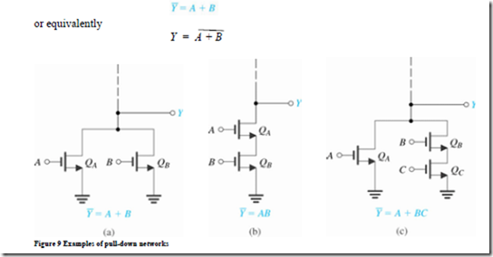
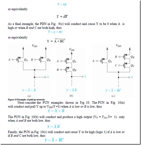
The PDN and the PUN each utilizes devices in parallel to form an OR function, and devices in series to form an AND function. For the circuit in Fig. 9(a), we observe that QA will conduct when A is high(VA=VDD) and will then pull the output node down to ground (VY=0V, Y = 0). Similarly, QB conducts and pulls Y down when B is high. Thus Y will be low when A is high or B is high, which can be expressed as
The PDN in Fig. 9(b) will conduct only when A and B are both high simultaneously.
Thus Y will be low when A is high and B is high,
Fig 11 shows our usual symbols (left) and the corresponding "digital" symbols (right). Observe that the symbol for the PMOS transistor with a circle at the gate terminal is intended to indicate that the gate terminal of the PMOS transistor is an active low input.
Remember that for an NMOS transistor, the drain is the terminal that is at the higher voltage(current flows from drain to source), and for a PMOS transistor the source is the terminal that is at the higher voltage (current flows from source to drain).
3.2 The Two-Input NOR Gate
Consider the CMOS gate that realizes the two-input NOR function
Y is to be low (PDN conducting) when A is high or B is high. Thus the PDN consists of two parallel NMOS devices with A and B as inputs (i.e., the circuit in Fig.9(a)).For the PUN, we note from the second expression in Eq. (19) that Y is to be high when A and B are both low. Thus the PUN consists of two series PMOS devices with A and B as the inputs (i.e., the circuit in Fig. 10(b)). Putting the PDN and the PUN together gives the CMOS NOR gate shown in Fig. 12.
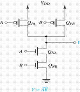
To synthesize the PDN, we consider the input combinations that require Y to be low: There is only one such combination, namely, A and B both high. Thus, the PDN simply Comprises two NMOS transistors in series (such as the circuit in Fig. 9(b)). To synthesize the PUN, we consider the input combinations that result in Y being high. These are found from the second expression in Eq. (20) as A low or B low. Thus, the PUN consists of two parallel PMOS transistors with A and B applied to their gates (such as the circuit in Fig. 10(a)). Putting the PDN and PUN together results in the CMOS NAND gate implementation shown in Fig. 13.
Figure 13 A two-input CMOS NAND gate
3.4 A Complex Gates
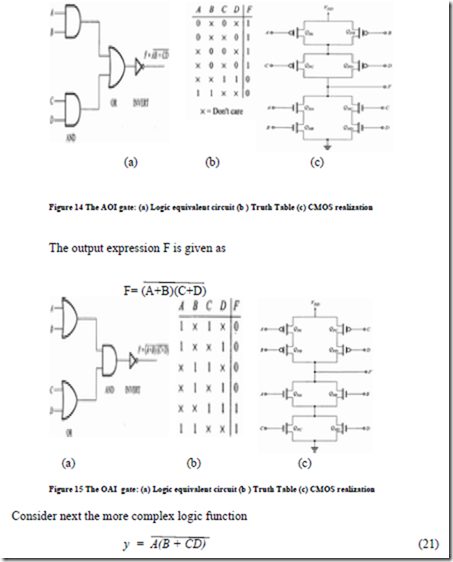
These are AND-OR-INVERT(AOI) and OR-AND-INVERT(OAI) gates. Both the complex gates have a propagation delay equivalent to that of a single NAND or NOR gate.
Let us implement the function
Here, AB and CD are two AND functions and their sum is the OR function, which is finally Inverted. Thus F can be implemented as an AOI gate. Figure14(c) shows the CMOS realization of an AOI gate. The truth table for this gate and its logic Equivalent circuit for the AOI gate are shown in figs.14(b) and 14(a), respectively.
The CMOS realization of the OR-AND-INVERT(OAI)gate is the dual of that for the AND-OR- INVERT(AOI) gate and is easily obtained by flipping that latter end-for-end while interchanging all NMOS circuits with PMOS circuits and vice versa, as shown in fig. 15(c). The truth table for this gate and its logic Equivalent circuit for the OAI gate are shown in figs.15(b) and 15(a), respectively.
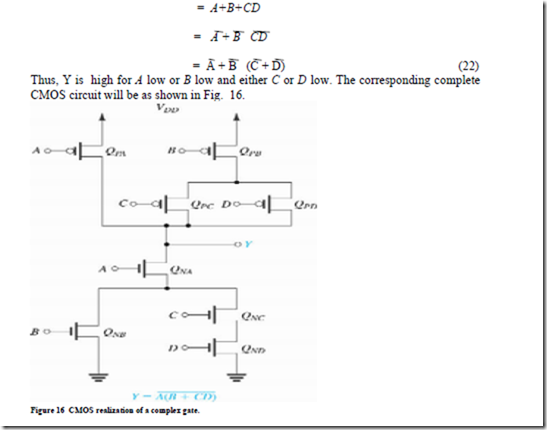
Since Y = A(B + CD), we see that Y should be low for A high and simultaneously either B high or C and D both high, from which the PDN is directly obtained. To obtain the PUN, we need to express Y in terms of the complemented variables. We do this through repeated application of DeMorgan's law, as follows:
3.5 Obtaining the PUN from the PDN and Vice Versa
From the CMOS gate circuits considered thus far (e.g., that in Fig. 16), we observe that the PDN and the PUN are dual networks: Where a series branch exists in one, a parallel branch exists in the other. Thus, we can obtain one from the other, a process that can be simpler than having to synthesize each separately from the Boolean expression of the function.
3.6 The Exclusive-OR Function
An important function that often arises in logic design is the exclusive-OR (XOR) function,
We observe that since Y (rather than Y) is given, it is easier to synthesize the PUN. We note, however, that unfortunately Y is not a function of the complemented variables only (as we would like it to be). Thus, we will need additional inverters. The PUN obtained directly from Eq. (23) is shown in Fig. 17(a). Note that the Q1, Q2 branch
realizes the first term (A B), whereas the Q3, Q4 branch realizes the second term(AB).
As for synthesizing the PDN, we can obtain it as the dual network of the PUN in Fig. 17(a). Alternatively, we can develop an expression for Y and use it to synthesize the PDN. DeMorgan’s law can be applied to the expression in Eq. (23) to obtain Y as
The corresponding PDN will be as in Fig. 17(b), which shows the CMOS realization of the exclusive-OR function except for the two additional inverters.
3.7 Summary of the Synthesis Method
1. The PDN can be most directly synthesized by expressing Y as a function of the uncomplemented variables. If complemented variables appear in this expression, additional inverters will be required to generate them.
2. The PUN can be most directly synthesized by expressing y as a function of the complemented variables and then applying the uncomplemented variables to the gates of the PMOS transistors. If uncomplemented variables appear in the expression, additional inverters will be needed.
3. The PDN can be obtained from the PUN (and vice versa) using the duality property.
3.8 Transistor Sizing
Once a CMOS gate circuit has been generated, the only significant step remaining in the design is to decide on W/L ratios for all devices. These ratios usually are selected to provide the gate with current-driving capability in both directions equal to that of the basic inverter, The reader will recall from Section 4 that for the basic inverter
design, we denoted (W/L)n = n and (W/L)p, = p, where n is usually 1.5 to
2 and, for a matched design, p =(µn/µP)n.Thus, we wish to select individual W/
L ratios for all transistors in a logic gate so that the PDN should be able to provide a
capacitor discharge current at least equal to that of an NMOS transistor with W/L = n, and the PUN should be ahle to provide a charging current at least equal to that of a PMOS transistor with W/L = p. This will guarantee a worst-case gate delay equal to that of the basic inverter.
"worst case" means that in deciding on device sizing, we should find the input combinations that result in the lowest output current and then choose sizes that will make this current equal to that of the basic inverter. The issue of determining the current-driving capability of a circuit consisting of a number of MOS devices. In other words, we need to find the equivalent W/L ratio of a network of MOS transistors.
consider the parallel and series connection of MOSFETs and find the equivalent W/L ratios.The derivation of the equivalent W/L ratio is based on the fact that the on resistance of a MOSFET is inversely proportional to W/L. Thus, if a number of MOSFETs having ratios of (W/L)1, {W/L)2, ... are connected in series, the equivalent series resistance obtained by adding the on-resistances will be
As an example, two identical MOS transistors with individual W/L ratios of 4 result in an equivalent W/L of 2 when connected in series and of 8 when connected in parallel.
Figure 18 Proper transistor sizing for a four-input NOR gate. Note that n and p denote the (W/L) ratios of QN and QP, respectively, of the basic inverter
As an example of proper sizing, consider the four-input NOR in Fig. 18. Here, the worst case (the lowest current) for the PDN is obtained when only one of the NMOS transistors is conducting. We therefore select the W/L of each NMOS transistor to be equal to that of the NMOS transistor of the basic inverter, namely, n. For the PUN, however, the worst- case situation (and indeed the only case) is when all inputs are low and the four series PMOS transistors are conducting. Since the equivalent W/L will be one-quarter of that of each PMOS device, we should select the W/L ratio of each PMOS transistor to be four times that of QP of the basic inverter, that is, 4p.
As another example, we show in Fig. 19 the proper sizing for a four-input NAND gate. Comparison of the NAND and NOR gates in Figs. 18 and 19 indicates that because p is usually two to three times n, the NOR gate will require much greater area than the NAND gate. For this reason, NAND gates are generally preferred for implementing combinational logic functions in CMOS.
3.9 Effects of Fan-In and Fan-Out on Propagation Delay
Each additional input to a CMOS gate requires two additional transistors, One NMOS and one PMOS. This is in contrast to other forms of MOS logic, where each additional input requires only one additional transistor. The additional transistor in CMOS not only increases the chip area but also increases the total effective capacitance per gate and in turn increases the propagation delay. The size-scaling method described earlier compensates for some(but not all) of the increase in tp. By increasing device size, we are able to preserve the current-driving capability.
The capacitance C increases because of both the increased number of inputs and increase in device size. Thus tP will still increase with fan-in, a fact that imposes a practical limit on the fan-in of, say, the NAND gate to about 4.
An increase in a gate’s fan-out adds directly to its load capacitance and, thus, increases its propagation delay.
Thus although CMOS has many advantages, it does suffer from increased circuit complexity when the fan-in and fan-out are increased, and from the corresponding effects of this complexity on both chip area and propagation delay.








Comments
Post a Comment