MOS Field-Effect Transistors (MOSFETs)part2
Transistor Q1, whose drain is shorted to its gate and thus is operating in the saturation region, such that
Where we have neglected channel-length modulation (i.e., assumed λ=0)
• The drain current of Q1 is supplied by VDD through resistor R. Since the gate currents are zero,
R is considered to be the reference current of the current source and is denoted IREF.
Now consider transistor Q2: It has the same VGS as Q1; thus if we assume that it is operating in saturation, its drain current, which is the desired current I of the current source, will be
where we have neglected channel-length modulation.
Equation (4.51) and (4.52) enable us to relate the current I to the reference current IREF,
This circuit, known as a current mirror, is very popular in the design of IC MOS amplifiers.
4.6 SMALL-SIGNAL OPERATION AND MODELS
In Section 4.4 we learned that linear amplification can be obtained by biasing the MOSFET to operate in the saturation region and by keeping the input signal small.
4.6.1 The DC Bias Point
The dc bias current can be found by setting the signal vgs to zero; thus,
The dc voltage at the drain, VDS or simply VD (since S is ground), will be
To ensure saturation-region operation, we must have
Furthermore, since the total voltage at the drain will have a signal component superimposed on VD, VD has to be sufficiently greater than VD -Vt to allow for the required signal swing.
Figure 4.34 Conceptual circuit utilized to study the operation of the MOSFET as a small- signal amplifier.
4.6.2 The Signal Current in the Drain Terminal
• The first term on the right-hand side of Eq.(4.57) can be recognized as the dc bias current ID (Eq. 4.54).
• The second term represents a current component that is proportional to the input signal vgs.
• The third term is a current component that is proportional to the square of the input signal.
Figure 4.35 presents a graphical interpretation of the small-signal operation of the enhancement MOSFET amplifier.
Figure 4.35 Small-signal operation of the enhancement MOSFET amplifier.
4.6.3 The Voltage Gain
Returning to the circuit of Fig. 4.34, we can express the total instantaneous drain voltage vD as follows:
The signal component
Note:
1. Gain is negative indicating 1800 phase shift between input and output
2. Gain is proportional to load resistance RD and transconductance gm
Figure 4.36 Total instantaneous voltages vGS and vD for the circuit in Fig 4.34
4.6.5 Small Signal Models for the MOSFET
FET behaves as a Voltage controlled current source – taking a signal vgs between gate and source and provides a current gmvgs at the drain terminal
Input and output resistances are very high ideally, infinite
Figure 4.37 Small-signal models for the MOSFET: (a) neglecting the dependence of iD on vDS in saturation
Exact Model
• The previous model assumes iD is independent of vDS which is not true, because of the effect of channel length modulation.
• This was modeled by a finite resistance r0 between drain and source, in parallel to the controlled current source typically of the order of 10kΩ to 100kΩ
Figure 4.37 Small-signal models for the MOSFET: (b) including the effect of channel- length modulation, modeled by output resistance ro = |VA| /ID.
The transconductance gm
• gm and r0 depend on the DC bias point of the circuit
• gm can be increased by by using a short and wide channel or by increasing the VGS
(which reduces the available voltage swing)
• We have the MOSFET transconductance parameter:
![clip_image040[4] clip_image040[4]](https://blogger.googleusercontent.com/img/b/R29vZ2xl/AVvXsEhPprDfBfCTVvPRgUWcqEktdFmlji-hzibmUp4CsomWHjHw3VN8l2EE0Zb5zF0dkbPol2lWzKv7hKj49Ur4Xqd1Zt5rZJn9VUWCxkEzm4bgGQJAUAkccHftzgsTiHxsPmp2sqLJh1H7yr8/?imgmax=800) Other useful expressions for gm - 1
Other useful expressions for gm - 1
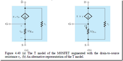
The T equivalent –Circuit Model
• The T model can be developed through a simple transformation of the previous hybrid –π model.
• This is very useful in many applications
Figure 4.39 Development of the T equivalent-circuit model for the MOSFET. For simplicity, ro has been omitted but can be added between D and S in the T model of (d).
· Figure 4.39(a) shows the equivalent circuit studied above without ro.
· In figure 4.39(b) we have added a second gmvgs current source in series with the original controlled source without causing any change in circuit operation.
· This newly created circuit node, labelled X, is joined to the gate terminal G in Fig 4.39(c). The gate current does’nt change, and remains at zero.
· A controlled current source gmvgs connected across its control voltage can be represented by a resistance as long as this resistance draws an equal current as the source. This replacement is shown in fig. 4.39(d).
The resistance between gate and source looking into the source is 1/gm, and the resistance as seen from the gate is infinite.
Alternate representation- VCCS by CCCS
Modeling the Body Effect
• When source and substrate are not shorted and substrate is tied to the most negative supply in the circuit, the body effect comes into picture and the substrate acts like a second gate for the MOSFET
• The signal Vbs gives rise to a drain current component, written as gmbvbs, where gmb is the body transconductance defined as
4.7 Single stage MOSFET Amplifiers
1. Common Source (CS) Amplifier :
A Common Source amplifier has the source terminal connected between the input and output. Input is applied between Gate –Source terminals and output is measured between the Drain-Source terminals. Any proper biasing method is used. Consider a CS amplifier with Constant current source biasing as shown below:
Figure 4.43 (a) Common-source amplifier
The ac equivalent circuit can be obtained by replacing the MOSFET with its small signal hybrid-π model and writing the remaining components between the respective terminals of the MOSFET in the model as shown below:
Figure 4.43 (b) Equivalent circuit of the amplifier for small-signal analysis. Now, the electro-mathematical analysis of the CS amplifier for the voltage gain (Av), Input impedance (Zin) and Output impedance (Zout) is as shown below:
Generally a Common Source amplifier will have a source resistance to improve the stability of the bias point. But this resistance also causes negative feedback and hence the voltage gain will be lesser than in a CS amplifier without source resistance.
Figure 4.44 (a) Common-source amplifier with a resistance RS in the source lead. The small signal equivalent circuit with ro neglected is as shown below:
49
Figure 4.44 Small signal equivalent model of Common Source amplifier with Rs From the figure we can see that as in the case of the CS amplifier,
But, here unlike the previous CS circuit, vgs is only a fraction of vi .It can be determined from the voltage divider composed of 1⁄gm and Rs that appears across the amplifier input as follows:
This shows that gain is reduced by a factor (1 + gm RS) than in the previous CS amplifier without RS.This factor is called the “amount of feedback” and that it determines both the magnitude of performance improvement and as a tradeoff, the reduction in gain. Since this RS was used to improve the stability under dc conditions, by reducing the variability of ID, for ac operation it has a similar action (reducing id), it is called “Source degeneration resistance”.
Another useful interpretation of the gain expression is that the gain from gate to drain is simply the ratio of the total resistance in the drain, (RD||RL) to the total resistance in the
Common Gate Amplifier [CG amplifier]
By applying a signal ground on the MOSFET gate terminal, a circuit configuration aptly named Common Gate or grounded gate amplifier is obtained. The input is applied between source and Gate and the Output is measured between the Drain and Gate. Since both the dc and ac voltages at the gate are zero, the gate terminal can be directly grounded as shown.
Since gm is of the order of 1mA/V, the input resistance of the CG amplifier is relatively low (of the order of 1kΏ) than in the CS amplifier.
Note:
· The CG amplifier is non inverting
· The input resistance of CG amplifier is very low.
· Voltage gain is smaller than that of a CS amplifier by factor (1+gmRsig) which is due to low Rin.
· This circuit also acts like a Unity gain current amplifier or a Current follower
· This is most commonly used in the Cascode amplifier.
Common Drain Amplifier (CD amplifier)
The signal ground is established at the drain terminal, input is given between the Gate and Drain terminals and Output is measured between the Source and Drain terminals as shown below:
Figure 4.46 (a) A common-drain or source-follower amplifier.
Here also, it is more convenient to use the small signal T-model for analysis, but including the resistance ro as shown below:
Figure 4.46 (b) Small-signal equivalent-circuit model.
Note:
· In source follower, Rin is independent of RL and Rout is independent of Rsig, due to zero gate current.
· Hence, it has a very high input resistance, very low output resistance and a voltage gain that is less than or close to unity.
· It is normally used as a buffer amplifier.
Summary:
· The CS amplifier is best suited for obtaining the bulk of the gain required in an amplifier. Depending on the gain required, either a single stage or a cascade of two or three stages is used.
· Including a resistor RS in the source terminal of the CS amplifier provides a number of improvements in its performance, as it behaves like an amplifier with negative Voltage series feedback amplifier, but at the expense of reduced gain.
· The low input resistance of the CG amplifier is used as unity gain current amplifier or current follower and also in Cascode amplifier.
· The source follower finds application as a voltage buffer for connecting a high resistance source to a low resistance load and as the output stage in a multistage amplifier.
PN: For SPICE MOSFET models and examples please refer to pages 446 to 453 in the text book Adel Sedra and K C Smith
4.2 Drain current is directly proportional to the width of the channel.Therefore if width is 10 times greater, then iD would be 10 times greater as well.
4.3 We know that
NOTE: PLEASE REFER TO ALL THE EXAMPLE PROBLEMS IN PRESCRIBED TEXT BOOK {SEDRA AND SMITH}
![clip_image002[5] clip_image002[5]](https://blogger.googleusercontent.com/img/b/R29vZ2xl/AVvXsEhk0MMYyePZQwPA23HNgrYCMoN_ynkpnkm3tsb8X_46JfrHSts0C7-wrg1rsh7rd8RlqYCjQvJvRao9z2LGSpP1cVlTFz90UyarStmpF0MM6fGT6abRfirasNVR8aO1u9u3jTXiAoueNHQ/?imgmax=800)
![clip_image004[4] clip_image004[4]](https://blogger.googleusercontent.com/img/b/R29vZ2xl/AVvXsEgQSi05t5kaEBBqG9tuuwoBs3LqdVTDFh-nFcV3c7_eLJfWFCMTPBVd37gNad4y8NGWBozYE8ewnh-XFPNLy2pXGABXauWQqy2qtEl9z24islqMRSBPp3WMMUwGxJJSBc446XwFFHY9N54/?imgmax=800)
![clip_image008[4] clip_image008[4]](https://blogger.googleusercontent.com/img/b/R29vZ2xl/AVvXsEivdCaEMcBGxhmoYxlmHWfohpdEGEX_kcZTcSI8OcyrbsA2Sq1FK0HR1BXLn8-3sgAgyZrkFILOkZB5veO9J3SxoPBBbh_RFS5Im6nPgemJHdiq5QLoH8Bd2raFCObXgjGYwJSN3wMzFuY/?imgmax=800)
![clip_image010[4] clip_image010[4]](https://blogger.googleusercontent.com/img/b/R29vZ2xl/AVvXsEhhmJwLSBV6WIk_5hWIm6D1kKc2rFzGDVDkzTXUILlsCPTCOKQPLB9ofcfXkLuvAeAUS9pUbNZRYQCprO6x8VAqUwzKzSjKjduPj9iCx4_bjxvpn7KMZPmsQaSd1X1n_IZYPHu-Kzks76w/?imgmax=800)
![clip_image016[4] clip_image016[4]](https://blogger.googleusercontent.com/img/b/R29vZ2xl/AVvXsEjHJd2Ko0kyfp9mR28jNS3DkoxNAEaLH2rAL2laZj-Y4n8kPxEhLB-4Lr07qMx1Dr5HSXEoBHMmuIeL7K25W9qmwE0Bi24FXPfSz9NaoQCNJ5V-LONr7z_clLrxKhXcqvYwT6scA_YsiHA/?imgmax=800)
![clip_image018[4] clip_image018[4]](https://blogger.googleusercontent.com/img/b/R29vZ2xl/AVvXsEi_sfedgZq4uHUT_ys2IMOnJv7FNWy0x6BWSwb-k63mBoa8cwqNsUeIYygYHlpTeglQU2eCSdFJ2HZjZ4DqrOPOhOz8OsMsSVorXjean3_ilF-m9CZoF4FjIg7cGAhl8B1DfRmlqo2Z3ho/?imgmax=800)
![clip_image020[4] clip_image020[4]](https://blogger.googleusercontent.com/img/b/R29vZ2xl/AVvXsEi9k-aacku95zzeifSigsk2PLhQMPADNb4lnnHwtTvOeCTxEs-BiWvo0L8A8JxIrXqxyyQI6Wp4TgnJRlnV1uXOMZ9rHssEQjwCmjGPgz1IpudbBLWw5QkKnvwNl9sl5jesBF_JCe04Wg0/?imgmax=800)
![clip_image022[4] clip_image022[4]](https://blogger.googleusercontent.com/img/b/R29vZ2xl/AVvXsEhoxRaEgfRG90TSfq3NXSuLu1t2kyvDbifu8XOQGKbOiY1Zh1r9NemgiPuxqrIoZX7kQlNXEmeXAYLCuaURlcTupC7O7pXzRWTGlINKpb4j-T7PAbRtK6aXSwuyJhgfXN7_gEpKIR2M8Fc/?imgmax=800)
![clip_image023[4] clip_image023[4]](https://blogger.googleusercontent.com/img/b/R29vZ2xl/AVvXsEi2Lm4U2ylPJJTiHs3xsRmECviivkQpEyHoI-s_Zo3IWjl7OZ3IDiqOHji4-Mkexn9HjE0rENCAwpgcDFVsj_qzJkEEuOiJyFauuXAPwhcFM8EEaW9N4Vk-Bo62XgcAVskIaX1KkQETtsM/?imgmax=800)
![clip_image026[4] clip_image026[4]](https://blogger.googleusercontent.com/img/b/R29vZ2xl/AVvXsEir21CsICU2tuY1COMMy-jvd3SCErYKiOk5lEtn6Pxec4yzaYv29yP-ElngTdsNry8VDPNIKMRTTGOmuXQYxoOTiqDp5r8zD_F9aEdNpJB02piUS0tLhkUCKImM4QKXKg9Y_tqwugmOq_s/?imgmax=800)
![clip_image028[4] clip_image028[4]](https://blogger.googleusercontent.com/img/b/R29vZ2xl/AVvXsEgOVqC27qgrsZbSCJZ41CR9xeM_1EESYWbykL0p9F9AcI3-vnHh5jNW25mCrUl_CErSArlbKgc20qkV50Sh6oXItBG_pV1yyapMlXqOHtsmfuRQk9UU9d4PVF2au-3lXA2cpxBvknwyrZE/?imgmax=800)
![clip_image030[4] clip_image030[4]](https://blogger.googleusercontent.com/img/b/R29vZ2xl/AVvXsEg9qUlS_p1FO4TcIXq2VyAssaYfTalgAVUJ_Jp3pUMv4E5fuyGMCItZdVq9QQzrQ4t4bo1wkVDYAEt0_WcqrGFMMeqax8S0gb9etryKl30ax1m1yA3RIHjEgMZjE_983gyabKb_20WsJbI/?imgmax=800)
![clip_image032[4] clip_image032[4]](https://blogger.googleusercontent.com/img/b/R29vZ2xl/AVvXsEiDPMFYvMojQZTxzGAX5YNVDombcL_9kiJmUTxIOLjreRb_jIn0px_XZ7-pooGcOXRtFq5tnmqdCoAn5LEN-NRVngMyBu8qmh0oXP254x7k7-MW4KTGGcN8zZRtQMTn9thtucxFnBa7DB0/?imgmax=800)
![clip_image034[4] clip_image034[4]](https://blogger.googleusercontent.com/img/b/R29vZ2xl/AVvXsEgPuS_EzbcIsleSMnDft-Nad8gDTQZwySDWRUvNOQVYnWFhB68cou1xzcgFY5UmBaPh5ZQz4CHqd6-MX0XF4e75iV3IixSoiGeqvPR51v7ab1ZXPOZ4g4tCKzET4e-OLQV0_PwukbLEJHo/?imgmax=800)
![clip_image042[4] clip_image042[4]](https://blogger.googleusercontent.com/img/b/R29vZ2xl/AVvXsEh7XNm4Q2ZTurPHq2l2-5ibb5FFJ5rcwpP_OH4eBiD7qYcdFLNjebCd2jd3FznQLFGiNVShoMidSqZ2YhLxFx0v3TSupDj7x_J7W-9TMVfMB3LSLt3sG4dhoQ34UujQcW60TmZ6zaDyEQI/?imgmax=800)
![clip_image044[4] clip_image044[4]](https://blogger.googleusercontent.com/img/b/R29vZ2xl/AVvXsEi5gs4cRhlrxMGfcfdr-dOKV1fsCvMij7Ac-jJMwatSO0eX2CZVc5G86dQiKYoDf4UskDV4bTofCmBXJoFZXpCvtjXU1lIVOeeyNhNUCdYvtpte063QYflhANlAU3qhkVf2Vvn0gKxeb0M/?imgmax=800)


![clip_image058[4] clip_image058[4]](https://blogger.googleusercontent.com/img/b/R29vZ2xl/AVvXsEhFMi67EyoWdcafbR_37dlJBQWSflbUWblZOTWRMhgh1OJnKOMiTQRDh9MLKTEKBcQGzbfQlX3uNSIPtko43JKqpJmAZXUM_8Idt0lEa3l9HKX7ZdGZ4rbakxOT19dqAJBbW1-LnKEDRuY/?imgmax=800)
![clip_image060[4] clip_image060[4]](https://blogger.googleusercontent.com/img/b/R29vZ2xl/AVvXsEiAyXKIvDiLe6obNM8otzcra466_JRspzpNXVZav22P9KvvfZN5J7QnQ0ZXyZ5rVpd_EAt0Tr3PqRLHBfN0D3V4rXyjYoYfdI2kPiPXZckufG22aoh_5XAAzAaERL1HQgYz8hCBkiERoX0/?imgmax=800)
![clip_image062[4] clip_image062[4]](https://blogger.googleusercontent.com/img/b/R29vZ2xl/AVvXsEjmhrEiht3XFr4FXb2jyPSF8HcHms11Qklpb_HLI6sKmhaPBWFcKNqwtPEyYL4L7bEjjtRb4sYdo1KlMpFIBCvIevyc2U_pRSXHtDcPoQB7k7TXCh18CIKt7WhMEpmoM26A33ps2MXwRsA/?imgmax=800)
![clip_image064[4] clip_image064[4]](https://blogger.googleusercontent.com/img/b/R29vZ2xl/AVvXsEicTNv-2e4gKCewDxNm51nDJwJNVvuC-UPfnsjB3DHtMHpHmxK9VLGNZsddr769iHVcNLjwhlhgEBREb9Owc4HoDwJwHrh4VsC5go20JrqY7gegc0UaTJwOJ2J7EOXlsnQzYkvwoCe8I20/?imgmax=800)
![clip_image066[4] clip_image066[4]](https://blogger.googleusercontent.com/img/b/R29vZ2xl/AVvXsEiRLIKXXP-ZR-umMsAXlv3ZQAvsNg-Y9CujGXc1DpT2EMHKbk29FnyuPLZltjlsYlAi1BENrXf6lIBglLkPT34Y2NIKWsjOtkezU53o7EIQ0wzxelFCFn3jYjUHCWChPOnEn1NakYLGByo/?imgmax=800)


![clip_image092[4] clip_image092[4]](https://blogger.googleusercontent.com/img/b/R29vZ2xl/AVvXsEgHRR13yg81NI1fs2igG3Naw6F9XFjVqqa_P4eMakH3LfOEXGYnm-jYb3y-J6r3fHUxdw5pIJGg0PphKhZwz7c_PqCqhRP3qGuP4ya_YC3tv_xbbNU8aL_clHQdk6pMl8Ga34j88RFsXtc/?imgmax=800)
![clip_image094[4] clip_image094[4]](https://blogger.googleusercontent.com/img/b/R29vZ2xl/AVvXsEiu__tBqzfb6GvPBxFPObB_z4UBM1nm3yjYI-E7Knt9zibU1vTY-RZp6X3JaGduB381z1Y8TuSgpzZp1_J96Lwup4Yj63g3yHehiei075gzUP_ecb5E-igAjJH9SqMrz71g3nwh8dcqozQ/?imgmax=800)


Comments
Post a Comment