Integrated-circuit amplifiers (contd.) part1
COMMON-SOURCE AND COMMON-EMITTER AMPLIFIERS
The Common-Source Circuit
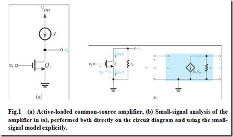
The most basic IC MOS amplifier is shown in fig.(1). The source of MOS transistor is grounded , also the drain resistor RD replaced by a constant-current source I. The current- source load can be implemented using a PMOS transistor and is therefore called an active load, and the CS amplifier of Fig. 1(a) is said to be active-loaded.
Before we consider the small-signal operation of the active-loaded CS amplifier, it is important to know that Q1 is biased to have ID = I. But the DC voltages at the drain and at the gate are developed by a circuit which is a part of a larger circuit in which negative feedback is utilized to fix the values of VDS and VGS. We shall assume that these circuits are in such a way that they bias the MOSFET in operate in the saturation region.
Since we analyse the circuit to obtain input impedance, voltage gain, current gain & output impedance in the view of small-signal, the biasing arrangement in the circuit is not shown. Small-signal analysis of the current-source-loaded CS amplifier is straightforward and is illustrated in Fig. 1(b). Here, along with the equivalent circuit model, we show the transistor with its r0 extracted and displayed separately and with the analysis performed directly on the circuit. From Fig. 1(b) we see that for this CS amplifier,
We note that |Avo| is the maximum voltage gain available from a common-source amplifier, namely the intrinsic gain of the MOSFET,
A0 = gmro
Common-Source Amplifier implemented using CMOS
A CMOS circuit implementation of the common-source amplifier is shown in Fig. 2(a) This circuit is based on that shown in Fig. 1(a) with the load current-source I implemented using transistor Q2. This is the output transistor of the current mirror formed by Q2 and Q3 and fed with the bias current IREF. We shall assume that Q2 and Q3 are matched; therefore the
i-v characteristic of the load device will be as shown in Fig. 2(b). This is simply the iD-vSD characteristic curve of the p-channel transistor Q2 for a constant source-gate voltage VSG. The value of VSG is set by passing the reference bias current IREF through Q3. Observe that, Q2 behaves as a current source when it operates in saturation, which in turn is obtained when v = vSD exceeds (VSG - |Vtp|), which is the magnitude of the overdrive voltage at which Q2 and Q3 are operating. Q2 exhibits a finite incremental resistance ro2, when it is in saturation and is given by,
Where VA2 is the Early voltage of Q2. In other words, the current-source load is not ideal but has a finite output resistance equal to the transistor r0.
The circuit’s transfer characteristic, vo versus vi, needs to be observed before analyzing the circuit to calculate voltage gain. This can be obtained using the graphical construction shown in Fig. 2 (c). Here we have sketched the iD-vDS characteristics of the amplifying transistor Q1 and superimposed the load curve on them. The latter is simply the i-v curve in Fig. 2(b) "flipped around" and shifted VDD volts along the horizontal axis. Now, since vGS1=vi, each of the iD-vDS curves corresponds to a particular value of vi. The intersection of each particular curve with the load curve gives the corresponding value of VDS1, which is equal to v0. Thus, in this way, we can obtain the v0-vi characteristic, point by point. The resulting transfer characteristic is sketched in Fig. 2(d). As indicated, it has four distinct segments, labeled I, II, III, and IV, each of which is obtained for one of the four combinations of the modes of operation of Q1 and Q2, which are also indicated in the diagram. Note also that we have labeled two important break points on the transfer characteristic (A and B) in correspondence with the intersection points (A and B) in Fig. 2 (c).
For amplifier operation segment III is the one of interest. Observe that in region III the transfer curve is almost linear and is very steep, indicating large voltage gain. In region III both the amplifying transistor Q1 and the load transistor Q2 are operating in saturation. The end points of region III are A and B: At A, defined by v0 = VDD - V0V2, Q2 enters the triode region, and at B, defined by v0 = vi – Vtn, Q1 enters the triode region. When the amplifier is biased at a point in region III, the small-signal voltage gain can be determined by replacing Q1 with its small-signal model and Q2 with its output resistances ro2. The output resistance of Q2 constitutes the load resistance of Q1. The voltage gain Av can be found from Eq. below
indicating that, as expected, Av will be lower in magnitude than the intrinsic gain of Q1, gm1ro1. For the case ro2 = rol, Av will be gm1rol/2.
The CMOS common-source amplifier can be designed to provide voltage gains ranging from 15 to 100. It offers a very high input resistance; however, its output resistance is also high.
Two final comments need to be made before leaving the common-source amplifier:
1. The circuit is not affected by the body effect since the source terminals of both Q1 and
Q2 are at signal ground.
2. The circuit is usually part of a larger amplifier circuit and negative feedback is utilized to ensure that the circuit in fact operates in region III of the amplifier transfer characteristic.
EXAMPLE
Consider the CMOS common-source amplifier in Fig. 2 (a) for the case VDD = 3 V, Vtn = |Vtp| = 0.6 V, µnC0X = 200 µA / V2, and µpC0x = 65 µA / V2. For all transistors, L = 0.4 µm and W=4 µm. Also, VAn = 20 V, | VAp|= 10 V, and IREF = 100 µA. Find the small- signal voltage gain. Also, find the coordinates of the extremities of the amplifier region of the transfer characteristic— that is, points A and B in the transfer characteristic.
Solution
Where | V0V3| is the magnitude of the overdrive voltage at which Q3 and Q2 are operating, and we have used the fact that, for Q3, VSD = VSG.
which is very close to the small-signal value of -42, indicating that segment III of the transfer characteristic is quite linear.
The Common-Emitter Circuit
The active-loaded common-emitter amplifier, in Fig. 3(a), is similar to the active-loaded common-source circuit studied above. Here also, the bias-stabilizing circuit is not shown. Small-signal analysis is similar to that for the MOS case and is shown in Fig. 3(b). The results are
which except for the rather low input resistance rπ are similar to the MOSFET case. Recall, however, from the comparison, that the intrinsic gain gmr0 of the BJT is much higher than that for the MOSFET. This advantage, however, is counterbalanced by the practically infinite input resistance of the common-source amplifier.
HIGH-FREQUENCY RESPONSE OF THE CS AND CE AMPLIFIERS
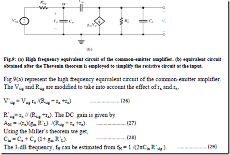
Consider the high-frequency response of the active-loaded common-source and common- emitter amplifiers. Figure4 shows the high-frequency equivalent circuit of the common- source amplifier. This equivalent circuit applies equally well to the CE amplifier with Cgs being replaced by Cπ, Cgd by Cµ, and Vgs by Vπ.
The input-signal source is represented by Vsig and Rsig. In some cases, Vsig and Rsig would be modified values of the signal-source voltage and internal resistance, taking into account other resistive components such as a bias resistor RG or RB, the BJT resistances rx and rπ, etc.
The load resistance RL represents the combination of an actual load resistance (if connected) and the output resistance of the current-source load. To avoid loss of gain; RL is usually of the same order as r0. We combine RL with r0, and denote their parallel equivalent R’L. The load capacitance CL represents the total capacitance between drain (or collector) and ground; it includes the drain-to-body capacitance Cdb (collector-to- substrate capacitance), the input capacitance of a succeeding amplifier stage, and in some cases, a deliberately introduced capacitance. In IC MOS amplifiers, CL can be relatively a very high value.
Analysis Using Miller's Theorem
When Rsig is relatively large and CL is relatively small. Miller's theorem can be used to obtain a quick but approximate estimate of the 3-dB frequency fH. Figure5 shows the approximate equivalent circuit obtained for the CS case, from which we see that the amplifier has a dominant pole formed by Rsig and Cin.
Analysis Using Open-Circuit Time Constants
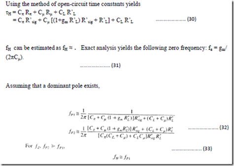
The method of open-circuit time constants can be applied to the CS equivalent circuit of Fig. 4, as illustrated in Fig. 6 from which we see that the resistance seen by Cgs, Rgs = Rsig and that seen by CL is R’L. The resistance Rgd seen by Cgd can be found by analyzing the circuit in Fig. 6(b) with the result that
In those cases in which CL is relatively high, this approach results in a better estimate of fH than that obtained using the Miller equivalence (because in the latter case we completely neglected CL).
Exact Analysis
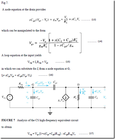
The approximate analysis presented above provides insight about the limit in high- frequency gain of the CS (and CE) amplifiers. Nevertheless, given that the circuit of Fig. 4 is relatively simple, it will be good if we perform an exact analysis. This is illustrated in
Fig.7.
We can now substitute in this equation for Vgs from Eq. (14) to obtain an equation in V0 and Vsig that can be arranged to yield the amplifier gain as
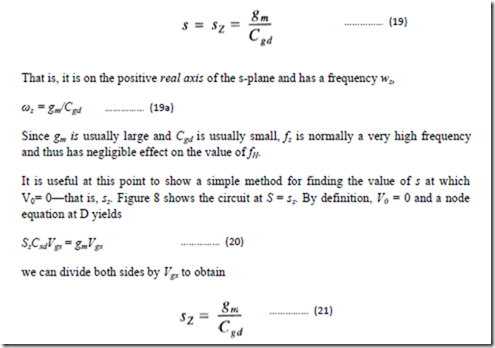
The transfer function in Eq. 18 indicates that the amplifier has a second-order denominator, and hence two poles. Now, since the numerator is of the first order, it follows that one of the two transmission zeros is at infinite frequency. This is readily verifiable by noting that as s approaches ∞, (V0 / Vsig) approaches zero. The second zero is at
We should note that in Eq. (18), as s goes toward zero, V0/Vsig approaches the dc gain (-gmR’L) as should be the case. In the denominator polynomial, we observe that the coefficient of the s term is equal to the effective time-constant τH obtained using the open-circuit time-constants method as given by Eq. (11).
 Fig8: The CS Ckt, at s=sz the output voltage Vo=0.
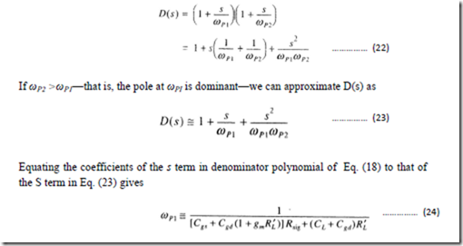
Denoting the frequencies of the two poles ωp1 and ωp2, we can express the denominator polynomial D(s) as
where the approximation is that involved in Eq. (18). Note that the expression in Eq. (24) is identical to the result obtained using open-circuit time constants and a little different from the result obtained using the Miller equivalence, the difference being the term (CL + Cgd)R’L related to the capacitance at the output, which was ignored in the original (simple) Miller derivation. Equating the coefficients of s2 in Eqs. (18) and (23), and using Eq. (24), frequency of the second pole:
EXAMPLE
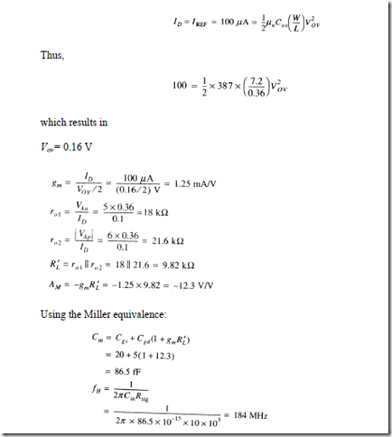
A CMOS common-source amplifier of the type shown in Fig. 2(a) has W/L = 7.2 µm/ 1.36 µm for all transistors, µn C0x = 387 µA/V2, npCox = 86 µA/ V2, IREF = 100 µA, V'An = 5 V/µm and | V'Ap| = 6 V/µm. For Q1, Cgs = 20 fF, Cgd = 5 fF, CL = 25 fF. and Rsig = 10kW. Assume that CL includes all the capacitances introduced by Q2 at the output node. Find fH using both the Miller equivalence and the open-circuit time constants. Also, determine the exact values of fP1, fP2, and fz and hence provide another estimate for fH.
Solution
Using the open-circuit time-constants method:
We note that this is about 25% lower than the estimate obtained using the Miller equivalence. The discrepancy is mostly a result of neglecting CL in the Miller approach. Note that CL here has a substantial magnitude and that its contribution to τH is significant (246 ps of the total 1160 ps, or 21%).
To determine the exact locations of zero and the poles, we use the transfer function in eq(18) .
The frequency of the zero is given by eq(19a) :
fz = gm/(2πCgd) = 40 GHz.
The frequencies wp1 and wp2 are found as the roots of the equation obtained by equating
the denominator polynomial of eq(18) to zero:
1 + 1.16 X 10⁻⁹s + 0.0712 X 10⁻¹⁸ s2 =0 and, the result is fp1 = 145.3 MHz
The Situation When Rsig is Low
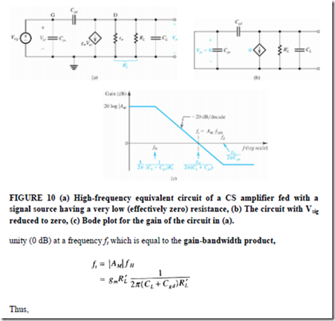
In the applications where the CS amplifier is fed with a low-resistance signal source, the high-frequency gain will no longer be limited by the source resistance and the input capacitance. The high-frequency limitation happens at the amplifier output, as shown below:
Figure 10(a) shows the high-frequency equivalent circuit of the common-source amplifier in when Rsig is zero. The voltage transfer function Vo/VSig = Vo/Vgs can be found by setting Rsig = 0 in Eq. (18). The result is
Thus, while the dc gain and the frequency of the zero do not change, the high-frequency response is now determined by a pole formed by CL + Cgd together with R'L. Thus the 3- dB frequency is now given by
To see how this pole is formed, refer to Fig. 10(b), which shows the equivalent circuit with the input signal source set to zero. Observe that the circuit reduces to a capacitance (CL + Cgd) in parallel with a resistance R'L.
As we have seen above, the transfer-function zero is usually at a very high frequency and thus does not play a significant role in shaping the high-frequency response. The gain of the CS amplifier will therefore fall off at a rate of-6 dB/octave (-20 dB/decade) and reaches
Example: Consider the CS amplifier specified when fed with a signal source having a negligible resistance (i.e. Rsig = 0). Find AM, f3dB, ft , and fz. If the amplifying transistor is to be operated at twice the original overdrive voltage while Wand L remain unchanged, what value of IREF is needed? What are the new values of AM , f3dB, ft and fz ?
Solution
We note that doubling Vov results in reducing the dc gain by a factor of 2 and increasing the bandwidth by a factor of 4. Thus, the gain-bandwidth product is doubled.
THE COMMON-GATE AND COMMON-BASE AMPLIFIERS WITH ACTIVE LOADS
The Common-Gate Amplifier
Figure 11(a) represents the basic IC MOS common-gate amplifier. The transistor has its gate grounded and its drain connected to an active load, given as an ideal constant- current source I. The input signal source vsig with a generator resistance Rs is connected to the source terminal. The MOSFET source is not connected to the substrate, hence the substrate terminal, B, is shown explicitly and indicate that it is connected to the lowest voltage in the circuit, i.e., to ground in this case. We may observe that except for showing the current-source I, which determines the dc bias current ID of the transistor, no other bias detail is shown. How the DC voltage VGS will be established and how VDS is determined are not of concern to us here. However, it should be known that bias stability is assured through the application of negative feedback to the larger circuit of which the CG amplifier is a part. In this case, we assume that the MOSFET is operating in the saturation region and concentrate exclusively on its small-signal operation.
The Body Effect: Since the substrate (i.e. body) is not connected to the source, the body effect plays a role in the operation of the common-gate amplifier. However, it turns out, that considering the body effect in the analysis of the CG circuit is very simple.
FIGURE 11 (a) Active-loaded common-gate amplifier, (b) MOSFET equivalent circuit for the CG case in wn.ch the body and gate terminals are connected to ground, (c) Small-signal analysis performed directly on the circuit diagram with the T model of (b) used implicitly, (d) Operation with the output open-circuited.
Recall that the body terminal acts, in effect, as a second gate for the MOSFET. Thus, just as a signal voltage vgs between the gate and the source gives rise to a drain current signal gmvgs, a signal voltage vbs between the body and the source gives rise to a drain current signal gmbvbs. Thus the drain signal current becomes (gmvgs + gmbvbs) where the body transconductance gmb is a small fraction χ of gm ; gmb = χgm and χ = 0.1 to 0.2.
Since in the CG circuit of Fig. 11(a) both the gate and the body terminals are connected to ground, vbs = vgs, and the signal current in the drain becomes (gm + gmb)vgs. It follows that the body effect in the common-gate circuit can be fully accounted for by simply replacing gm of the MOSFET by (gm + gmb). As an example, Fig. 11(b) shows the MOSFET T-model modified in this way.
Small-Signal Analysis The small-signal analysis of the CG amplifier can be performed either on an equivalent circuit obtained by replacing the MOSFET with its T model of Fig. 11(b) or directly on the circuit diagram with the model used implicitly. The latter approach is opted in order to gain greater insight into circuit operation. Figure 11(c) shows the CG circuit prepared for small-signal analysis. Here we observe "extracted" r0 of the MOSFET and shown it separately from the device. The resistance 1 /(gm + gmb), which appears in effect between gate and source looking into the source is also indicated. Note that a resistance RL is shown at the output; it is assumed to include the output resistance of the current-source load I as well as any load resistance if connected.
The circuit of Fig. 11(c) is analysed to determine the various parameters that characterize the CG amplifier. The CG amplifier is not a unilateral circuit; the resistance rQ connects the output node to the input node. As a result we should expect the amplifier input resistance Rin to depend on RL and the output resistance Rout to depend on Rs.
Input Resistance To determine the input resistance Rin, we must find a way to express ii in terms of vi. Inspection of the circuit in Fig. 11(c) reveals a key observation. The input current ii splits at the source node into two components: the source current i = (gm + gmb) vi and the current through r0, iro These two components combine at the drain to constitute the current io supplied to RL, ; thus io = ii, and vo = i0RL = iiRL. Now we can write at the source node
Observe that for r0 = ∞, Rin reduces to 1 /(gm + gmb) which is indeed the input resistance with r0 neglected. When r0 is taken into account, this value of input resistance is obtained approximately only for RL = 0. For the usual case of RL = ro, Rin = 2/(gm + gmb). Interestingly, for large values of RL approaching infinity, Rin = ∞.
Operation with RL = ∞ Figure 11(d) shows the CG amplifier with RL removed; that is, RL = ∞ and the amplifier is operating with the output open-circuited. We note that since io=0, ii, must also be zero; the current i in the source terminal, i = (gm + gmb)vi, simply flows via the drain through ro and back to the source node. It follows that the input resistance with no load, Ri, is infinite:
This is a very important quantity that appears in almost all formulas that characterize the CG amplifier. We observe that Avo differs from the intrinsic gain of the MOSFET in two minor respects: First, there is an additional term of unity, and second, gmb is added to gm. Typically Avo is 10% to 20% larger than A0.
We should also note that the gain of the CG circuit is positive. That is, unlike the CS amplifier, the CG amplifier is non-inverting.
From Eqs. (39) and (41), we can express the input resistance of the CG amplifier in the form as shown:
That is, the CG circuit divides the total resistance (ro + RL) by the open-circuit voltage gain, which is approximately equal to the intrinsic gain of the MOSFET. Furthermore, since Avo= (gm + gmb)r0 ≡ A0, the expression for Rin can be simplified to
This expression says that taking r0 into account adds a component (RL/A0) to the input resistance. This additional component becomes significant only when RL is large.
Another interesting result that follows directly from the fact that ii = 0 in the circuit of Fig. 11(d): The voltage drop across Rs will be zero. Thus Vi = Vsig, and the open-circuit overall voltage gain, vo/vsig will be equal to Avo,
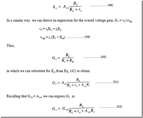
Voltage Gain The voltage gains Av and Gv of the loaded CG amplifier of Fig. 11(c) can be obtained in a number of ways. The most direct approach is to make use, once more, of the fact that io = ii and express v0 as
Output Resistance To complete our characterization of the CG amplifier, we find its output resistance. We recall that there are two different output resistances: Ro, which is the output resistance when vi is set to zero, and Rout which is the output resistance when vsig is set to zero. Both are illustrated in Fig. 12. Obviously R0 can be obtained from the expression for Rout by setting Rs = 0. It is important to be clear on the application of Ro and of Rout. Since R0 is the output resistance when the amplifier is fed with an ideal source vi it follows that it is the applicable output resistance for determining Av from Avo,
On the other hand, Rout is the output resistance when the amplifier is fed with vsig and its resistance Rs; so it is the applicable output resistance for determining Gv from Gvo,
A verification of this result is achieved by substituting Ro = ro in Eq. (53) and then observing that the resulting expression for Av is identical to that in Eq. (48), which we obtained from circuit analysis.
Utilizing the analysis indicated on the circuit diagram in Fig. 12(b), we can write for vx
Equations (56) and (57) can be combined to eliminate v and obtain vx in terms of ix and hence Rout = vx/ix.
We recognize the term multiplying Rs as the open-circuit voltage gain Avo; thus Rout can be expressed in an alternative, more compact form as
A verification of the formula for Rout in Eq. (59) can be obtained by substituting it in Eq. (54). The result will be seen to be identical to the gain expression in Eq. (52), which we derive by circuit analysis.
The expressions for Rout in Eqs. (58) and (59) are very useful results that we will employ frequently further. These formulas give the output resistance not only of the CG amplifier but also of a CS amplifier with a resistance Rs in the emitter.
A first interpretation, immediately available from Eq. (59), is that the CG transistor increases the output resistance by adding to r0 a component Avo Rs . In many cases the latter component would dominate, and one can think of the CG MOSFET as multiplying the resistance Rs in its source by Avo, which is approximately equal to gmr0.
Note that this action is the complement of what we saw earlier in regard to Rin where the MOSFET acts to divide RL by Avo. This impedance transformation action of the CG MOSFET is illustrated in Fig. 13 and is a key to number of applications of the CG circuit.
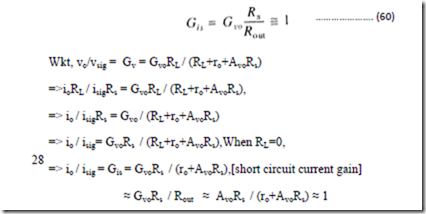
One such application involves the use of the CG amplifier as a current buffer. Fig. 14 shows an equivalent circuit that is suitable for such an application. It can be shown that the overall short-circuit current gain Gis is given by
The near-unity current gain together with the low input resistance and high output resistance are all characteristics of a good current buffer.Yet another interpretation of the formula for Rout can be obtained by expressing Eq. (58) in the form
Thus placing a resistance Rs in the source lead, results in multiplying the transistor output resistance ro by a factor (1+gmRs).
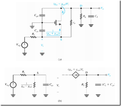
High-Frequency Response Figure 15(a) shows the CG amplifier with the MOSFET internal capacitances Cgs and Cgd indicated. For generality, a capacitance CL is included at the output node to represent the input capacitance of a succeeding amplifier stage. Capacitance CL also includes the MOSFET capacitance Cdb. Note the CL appears in effect in parallel with Cgd. Therefore, in the following discussion we will lump the two capacitances together.
It is important to note that each of the three capacitances in the circuit of Fig. 15(a) has a grounded node. Hence none of the capacitances undergoes the Miller-multiplication effect seen in the CS stage. It follows that the CG circuit can be designed to have a much wider bandwidth than that of the CS circuit, especially when the resistance of the signal generator is large.
FIGURE 15 (a) The common-gate amplifier with the transistor internal capacitances shown. A capacitance CL is also included, (b) Equivalent circuit for the case in which ro is neglected.
Analysis of the circuit in Fig. 15(a) is greatly simplified if ro can be neglected. In such a case the input side is isolated from the output side, and the high-frequency equivalent circuit takes the form shown in Fig. 15(b). We immediately observe that there are two poles: one at the input side with a frequency fP1
and the other at the output side with a frequency fP2.

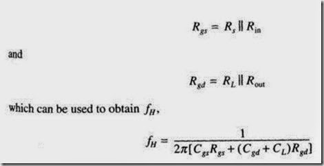
In situations when ro has to be taken into account (because Rs and RL are large), the method of open-circuit time constants can be employed to obtain an estimate for the 3-dB frequency fH ,Fig.16 shows the circuits for determining the resistances Rgs and Rgd seen by Cgs and (Cgd + CL), respectively. By inspection we obtain
It can be noticed that this circuit performs well as a current buffer, raising the resistance level from Rin= 4 kW to Rout = 300 kW and having an overall short-circuit current gain of 0.94 A/A. Because of the high output resistance, the amplifier bandwidth is determined mainly by the capacitance at the output node. So, additional load capacitance can lower the bandwidth significantly.
Exercise:
a) For the CG amplifier considered in Example above, find the value of fH when a capacitance CL = 5 fF is connected at the output.
Ans. 196 MHz
b) Repeat the problem in above Example for the case Rs = 1 kW and RL = 10 kW .
Ans. Avo = 28 V/V; Rin = 1 kW; Rout = 46 kW; Gv = 5 V/V; Gis = 0.61 A/A;
Gi = 0.5 A/A; fH= 2.61 GHz

















Comments
Post a Comment